A highly efficient dual-mode linear CMOS stacked-FET power amplifier (PA) is implemented for 3G UMTS and 4G LTE handset applications. High efficiency is achieved at a backed-off output power (Pout) below 12 dBm by employing an active-bypass amplifier, which consumes very low quiescent current and has high load-impedance. The output paths between high- and low-power modes of the PA are effectively isolated by using a bypass switch, thus no RF performance degradation occurs at high-power mode operation. The fabricated 900 MHz CMOS PA using a silicon-on-insulator (SOI) CMOS process operates with an idle current of 5.5 mA and shows power-added efficiency (PAE) of 20.5%/43.5% at Pout = 12.4 / 28.2 dBm while maintaining an adjacent channel leakage ratio (ACLR) better than –39 dBc, using the 3GPP uplink W-CDMA signal. The PA also exhibits PAE of 35.1% and ACLRE-UTRA of –33 dBc at Pout = 26.5 dBm, using the 20 MHz bandwidth 16-QAM LTE signal.
As a mobile communication standard is evolved toward 3G UMTS and 4G LTE, the importance of power amplifier (PA) efficiency is growing to extend the battery lifetime of mobile terminals [1]. The explosive demand for high-speed data transmission has now led handset PA researchers to focus on improvement of efficiency at high power levels, since 4G LTE PAs cover a wide bandwidth signal (10–20 MHz) and are mostly operated in the high output power region (>24 dBm) to maximize the data rate. The efficiency enhancement at lowpower level (< 12 dBm) also remains important for extending talk-time of the voice-centric 2G/3G standards (backward compatibility); thus, this should be applied to PAs [1].
To enhance the efficiency in the low output power (
Recent CMOS technology has also played an important role in handset PA design due to its size and cost benefits. By employing several power combining techniques such as the differential cascode and stacked-FET structures, the breakdown issue of a CMOS device is avoided and thus CMOS PAs are able to deliver watt-level
The authors’ previous work [8] introduced a highly efficient stacked-FET linear CMOS PA using an active full-bypass for 3G handset applications. This paper expands the work [8] by presenting a detailed design description (in Section II) and fabrication and measurement results, including the 20 MHz bandwidth 4G LTE as well as the 3G W-CDMA (in Section III).
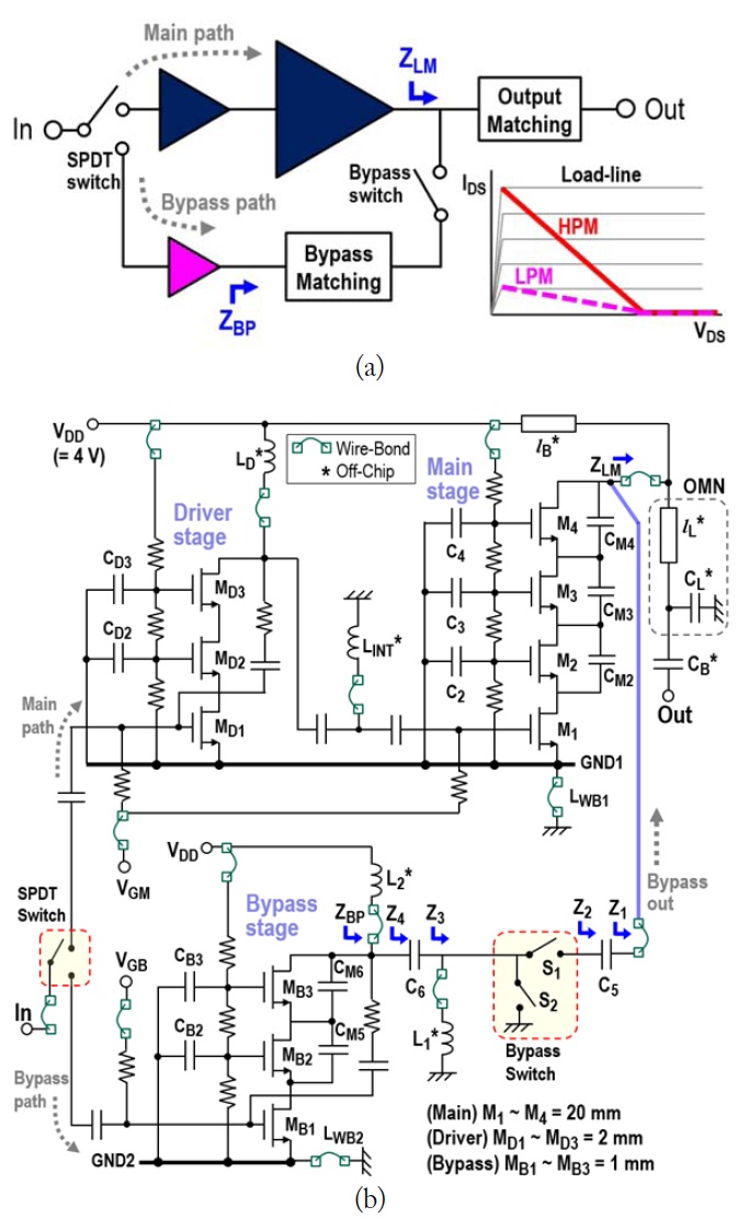
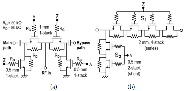
Fig. 1(a) shows a block diagram of the proposed dual-mode linear CMOS stacked-FET PA. It consists of a two-stage main amplifier and a bypass amplifier, each aiming for high-power mode (HPM) and low-power mode (LPM) amplification. Since both amplifiers share an identical supply voltage, the load impedance of the bypass amplifier,
The detailed schematic of the proposed PA is shown in Fig. 1(b). The PA design is based on a single-ended stacked-FET PA theory [5], where the main amplifier is composed of a triple-stack driver-stage (2 mm gate-width) and a quadruplestack main-stage (20 mm gate-width) for watt-level power amplification under
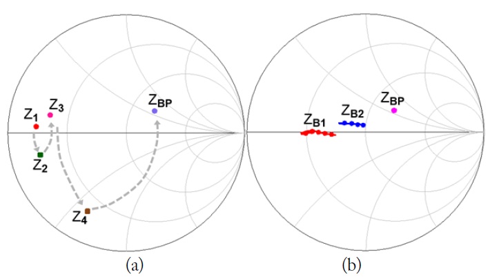
The efficiency during LPM operation is enhanced by designing the load impedance of the bypass-stage (
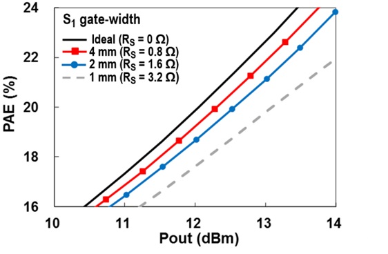
The input and bypass switches are designed based on the required insertion loss, isolation, and power handling. Since the input SPDT switch does not require high power handling and low loss, a simple single-stack series-shunt configuration is employed, as shown in Fig. 3(a). The simulated insertion loss and RF power handling of the SPDT switch are 0.1 dB and 19 dBm, respectively. On the other hand, the bypass switch experiences a high RF voltage swing during HPM and output thru-loss during LPM operation. Since the series-arm (
III. FABRICATION AND MEASUREMENT
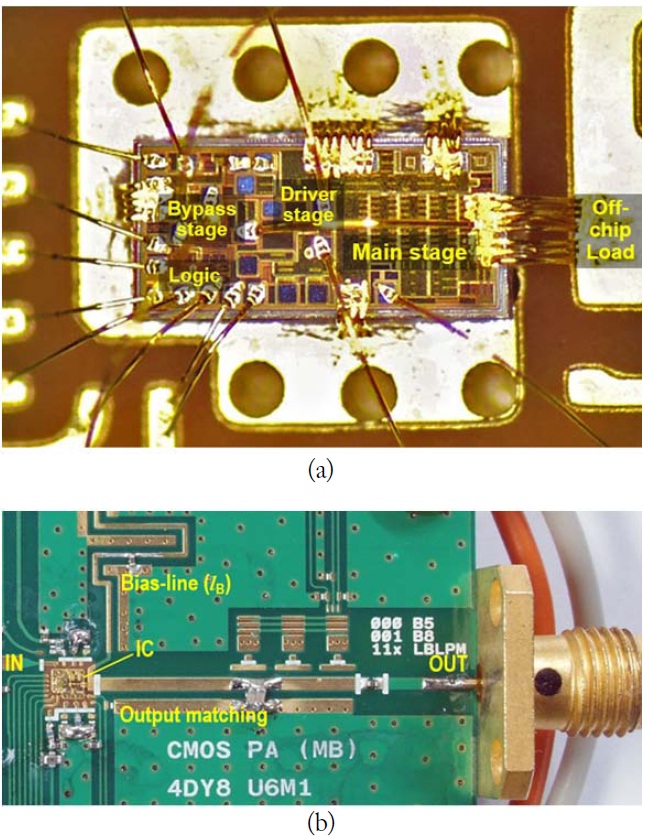
The designed PA was fabricated using a 0.18-μm silicon-oninsulator (SOI) CMOS process and all the MOSFETs used in this work have a gate-length of 0.32-μm (2.5-V device). A single NFET for RF switch offers a series resistance of 0.8 Ω and an off-capacitance of 310 fF/mm, resulting in figure-ofmerit of 250 fsec [10]. Capacitances of the seven gate capacitors for common-gate FETs,
The PA module was tested at 897.5 MHz (3G/4G Tx center frequency of band-8) and
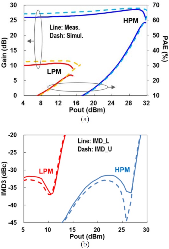
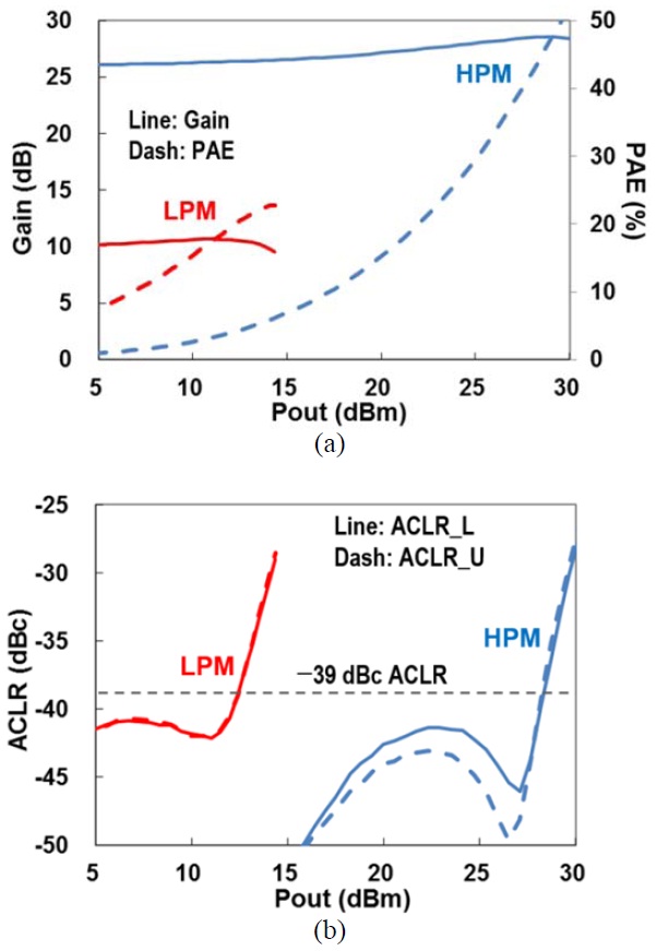
Measured W-CDMA (Rel’99) results of the PA are plotted in Fig. 7. During HPM operation, the PA showed a linear gain of higher than 26 dB and an adjacent channel leakage ratio (ACLR) better than –39 dBc up to
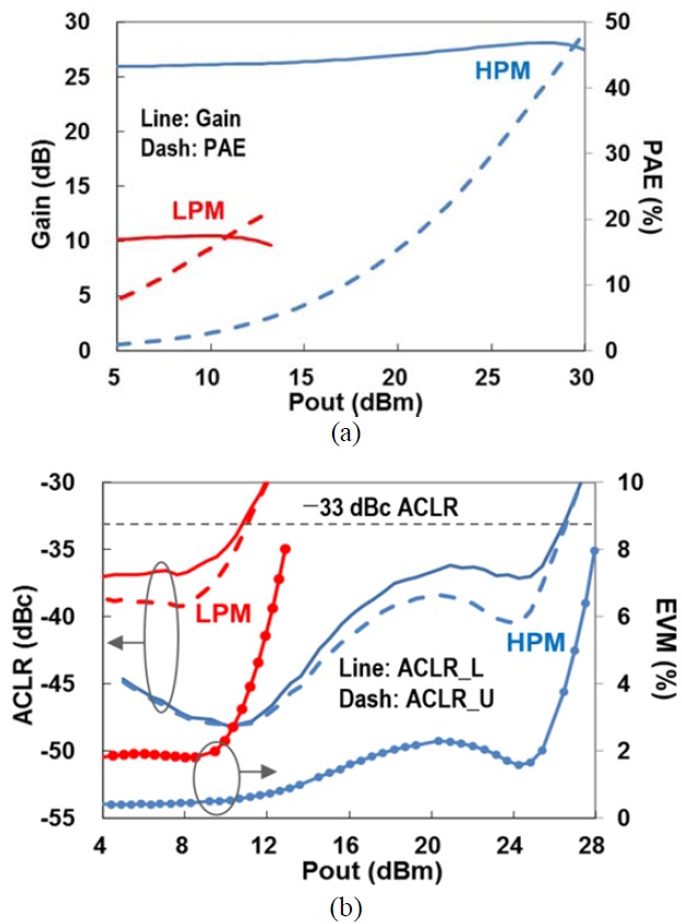
Finally, LTE performance was measured using the 20 MHz-bandwidth 16-QAM signal (peak to average power ratio [PA-PR] = 7.3 dB) and the result is plotted in Fig. 8. The signal was obtained from the Agilent’s Signal Studio (N7624B). The PA showed ACLRE-UTRA/error vector magnitude (EVM) of better than –33 dBc/3.8% up to
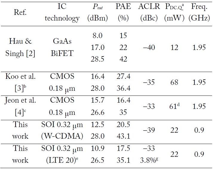
The performance of recently reported multi-mode W-CD-MA PAs is summarized in Table 1. Compared to the reported CMOS PAs, the proposed PA shows the lowest quiescent DC power (22 mW) and better linear efficiency below 12 dBm, thus resulting in a significant reduction on average current consumption. The linearity and efficiency of the proposed PA at both power modes are favorable among the reported CMOS PAs and are also comparable to the GaAs-based PAs.
[Table 1.] Performance comparison of recently reported multi-mode WCDMA PAs

Performance comparison of recently reported multi-mode WCDMA PAs
A 900 MHz dual-mode stacked-FET PA has been implemented using an SOI CMOS technology for 3G/4G handset applications. Employing an active-bypass amplifier and RF switches resulted in significant PAE improvement at low-power level while maintaining good RF performance at high-power region. The fabricated PA showed a PAE of 20.5%/43.5% and -CDMA ACLR of –39 dBc at