As monolithic microwave integrated circuit (MMIC) technology matures, applications that require power over a broad bandwidth are emerging at the millimeter-wave frequency range. Compact and reliable power sources that can replace the traditional Gunn oscillator-based method are desirable, and MMIC technology offers an attractive solution [1]. However, generating a millimeter-wave signal using an MMIC oscillator directly is very difficult. The electrical performance of MMICs is also poor compared to the Gunn oscillator. A frequency-multiplying method with low frequency signals below the Ka-band frequency is a very useful way to obtain millimeter-wave signals.
Until recently, many kinds of passive multipliers using diodes were the dominant components developed for use at millimeter-wave frequencies [2,3]. In general, active frequency multipliers are preferred because they offer lower conversion loss (or even conversion gain), wider bandwidth, and better isolation [4,5].
Multiplier MMICs with an output power of less than 0 dBm in the E-band frequency range are commercially available from Hittite and Agilent Technologies [5,6].
In this paper, we introduce a commercially fabricated frequency doubler MMIC that can be used to provide LO power of more than 13 dBm directly to mixers in an E-band heterodyne transceiver without a driver amplifier.
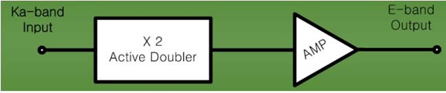
1. Configuration of E-band Frequency Doubler
The high output power of a frequency doubler MMIC that can pump a mixer without an additional driver amplifier is a preferred characteristic, as this can reduce the assembly loss and integration complexity in a millimeter-wave module. We adapted the combination of an active doubler and a buffer amplifier for the configuration of an E-band frequency doubler. The output buffer amplifier not only increases the output power of the signal but also isolates the doubler from changes in the load impedance. The simplified block diagram of the doubler configuration is shown in Fig. 1.
To satisfy the output power requirement of over 13 dBm, the active doubler and the amplifier should have an output power higher than 8 dBm and a gain of more than 5 dB over the operating frequency band, respectively.
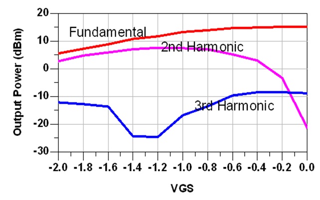
Even though the use of an accurate model of a high electron mobility transistor (HEMT) is the best way to design an active doubler, the four kinds of HEMT models optimized for amplifier design of class-A were available to us from the design kit. These HEMT models were composed of two kinds of drain voltages, 2 V and 4 V, and two kinds of drain currents, 150 mA/mm and 300 mA/mm. We need an HEMT to be able to generate the second harmonic signal over an 8 dBm output power from an input signal of 10 dBm. We selected an HEMT with 4 fingers and a total gate width of 120 μm (4F120) as an active doubler device, and an HEMT model of 4 V/150 mA after the simulation had been conducted under a pinch-off bias and an input power of 10 dBm. Fig. 2 shows the simulation results of a 4F120 HEMT under bias and input power conditions.
We also performed a power spectrum simulation for the HEMT device in order to find the optimal pinch-off bias for the active doubler, as shown in Fig. 2. The figure indicates an optimum gate voltage of -1.2 V to obtain the maximum second harmonic output and minimum third harmonic output simultaneously.
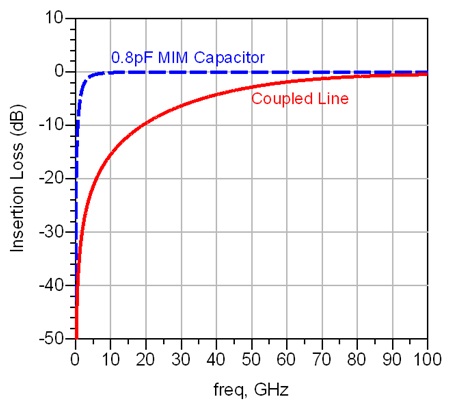
In a frequency doubler design, one or two open stubs are usually adapted to reject the output of the fundamental signal. In addition to the use of such stubs, we have used a coupled line section to enhance the fundamental uppression and implement the output-matching circuit of the active doubler. We used a characteristic in which the coupled line fitted at the second harmonic frequency has the nature to inherently suppress the fundamental frequency. The coupled line has been optimized for the active doubler to achieve the maximum fundamental suppression and a second harmonic output power of over 8 dBm. Fig. 3 shows the simulation results, in which the coupled line provides an additional rejection of more than 4 dB compared to a 0.8 pF metal-insulator-metal (MIM) capacitor over the input range. We can also expect an additional rejection for the fundamental signal to be added by using two coupled lines in the buffer amplifier. As we can see in Fig. 3, the coupled line is able to reduce the transmission of a signal below 10 GHz by more than 15 dB and it is therefore obvious that the coupled line can contribute greatly to enhancing the stability of an active doubler.
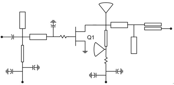
A radial stub and an open stub have been used to suppress unwanted harmonics at the output of the active doubler. A radial stub instead of a bypass capacitor in the E-band frequency range has been used in the drain bias circuit at the output of the active doubler. To enhance the stability of the active doubler, small resistors have been used at the gate terminal of the HEMT and in the drain bias circuit. The simplified schematic circuit of the active doubler is shown in Fig. 4.
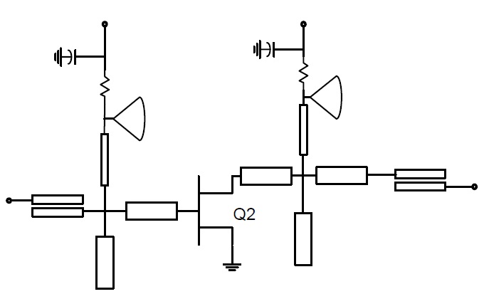
An HEMT with 4 fingers and a total gate width of 160 μm has been selected for the buffer amplifier design in order to achieve a P1dB performance of more than 15 dBm and a gain of more than 5 dB in an E-band frequency range after the nonlinear simulation of different kinds of class-A HEMT models in the model library.
As mentioned in the design description of the active doubler, the matching circuits were designed using two coupled lines together with open stubs at the input and output of the HEMT. Fig. 5 shows the implified schematic circuit of the buffer amplifier.
4. Design Result of E-band Frequency Doubler
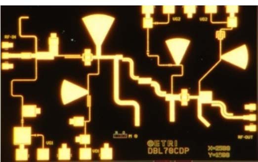
An inter-stage tuning process was conducted to optimize the pass-band conversion gain after the buffer amplifier was integrated with the designed active doubler. A photograph of the fabricated MMIC chip is shown in Fig. 6. Three microstrip coupled lines with curved shapes were used to reduce the chip size.
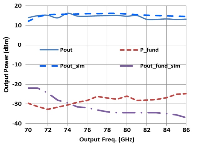
The MMIC was expected to have an output power of the second harmonic signal of more than 13 dBm over the frequency range of 71 to 86 GHz, and an output power of the fundamental signal less than -27 dBm over the input frequency range of 35 to 43 GHz. The input signal was driven at a power of 10 dBm.
We used an on-wafer probe station to test the performance of the fabricated doubler chip together with many kinds of millimeter-wave and microwave measurement equipment, such as a high power signal generator and spectrum analyzer with external V-band and W-band test mixers. The fabricated doubler measured the second harmonic output at 13 to 16 dBm over a frequency range of 71 to 86 GHz, and the fundamental leakage at less than -25 dBm under an input signal condition of 10 dBm over a frequency range of 35.5 to 43 GHz, as shown in Fig. 7. The measured output spectrum is very close to the simulated results.
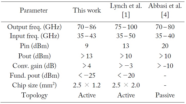
Table 1 shows a summary of the performances of the developed doubler MMIC compared with two previously reported multiplier chips [1,4].
[Table 1.] Performance comparison of E-band frequency doublers

Performance comparison of E-band frequency doublers
The over -13 dBm on-wafer measurement results of the output power for our doubler MMIC chip indicates sufficient performance to directly drive the mixers as a local signal for E-band transceiver applications. The operating frequency band of the doubler chip covers the frequency band for an E-band transceiver, as well as for 77-GHz car radar applications.