A planar transmission line with a dumbbell-shaped defected ground structure (DGS) provides low-pass transmission characteristics with a wide rejection frequency band. Due to the wideband rejection property, DGSs with a dumbbell shape are popularly used in the suppression of undesired harmonics for microwave and millimeter wave circuits and in the design of low-pass filters [1,2]. To date, the analysis of the dumbbellshaped DGS loaded planar transmission lines has almost always involved utilizing commercial electromagnetic full-wave solvers. The simulated
In this paper, we propose a new equivalent circuit model for a dumbbell-shaped DGS coupled to a transmission line, especially a microstirp line, to provide design rule and physical insight. Also, simple approximate expressions are presented to determine the main circuit parameters for this model.
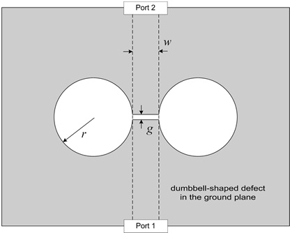
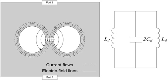
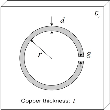
Fig. 1 illustrates the geometry of the microstrip line with a dumbbell-shaped DGS where two circular etched areas are connected by a narrow etched gap. In the DGS, the electric field is concentrated around the narrow etched gap while the current is confined to the metallic ground plane surrounding the circular etched pattern at resonance.
Hence the DGS in the ground plane can be represented by an LC resonant circuit model as shown in Fig. 2. Since there are two circular etched areas, two
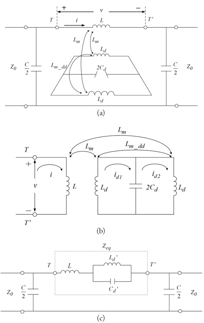
For the dumbbell-shaped DGS loaded microstrip line, the equivalent circuit model can be proposed as illustrated in Fig. 3(a). The magnetic flux from the current on the host transmitssion line passes through the wide etched circular area on the ground plane and it causes a magnetic coupling of the DGS to the host line. The
To obtain a simplified equivalent circuit of the DGS, the equivalent impedance of the branch between
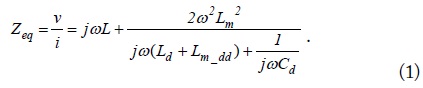
From (1), the complex circuit between

with the resonance angular frequency of At resonance,
since
III. PARAMETER EXTRACTION FOR EQUIVALENT CIRCUIT
One of the aims in this paper is to find values of parameters of the equivalent circuit model for the dumbbell-shaped DGS coupled to the microstrip line. In the patterned ground plane, the current distribution is confined within the metallic periphery of the circular etched pattern, as shown in Fig. 2. Hence the inductance
where
In Fig. 2, the capacitance of the DGS on the ground plane consists of the gap capacitance and the surface capacitance. The gap capacitance is calculated by the expression for the parallelplate capacitor of the gap with the correction due to the fringing fields. The surface capacitance is calculated by the analytical expression for the surface capacitance of a metallic split ring [4].
By replacing the air and substrate regions of the microstrip by a homogeneous medium with an effective permittivity
In (5) the first two terms are the expressions for the gap capacitance that accounts for the fringing effect [5], the third term is an analytical expression for the surface capacitance, and
In the DGS cell, since the inductance of the signal line is strongly coupled with the inductance of the split ring surrounding the etched area, the coupling coefficient
IV. SIMULATION AND EXPERIMENTAL RESULTS
Having extracted circuit parameters using the analytic expressions in the previous section,
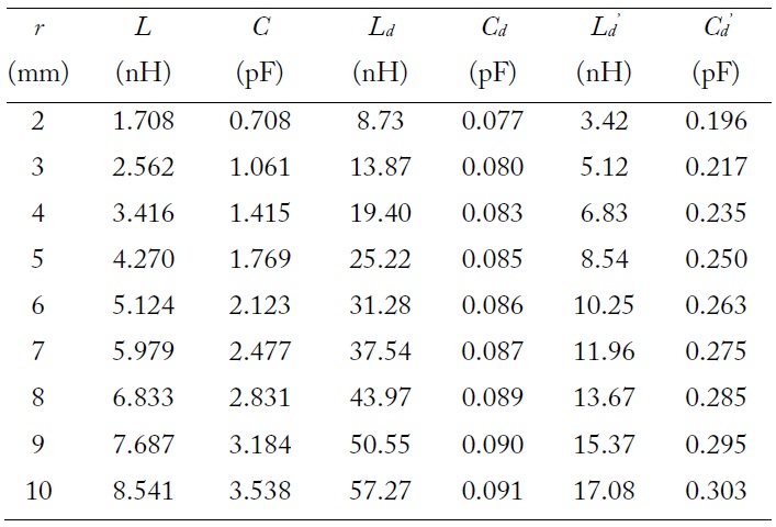
Extracted circuit parameters for various radii of the etched circular pattern (km = 1, km_dd = 0)
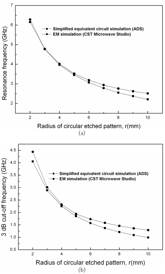
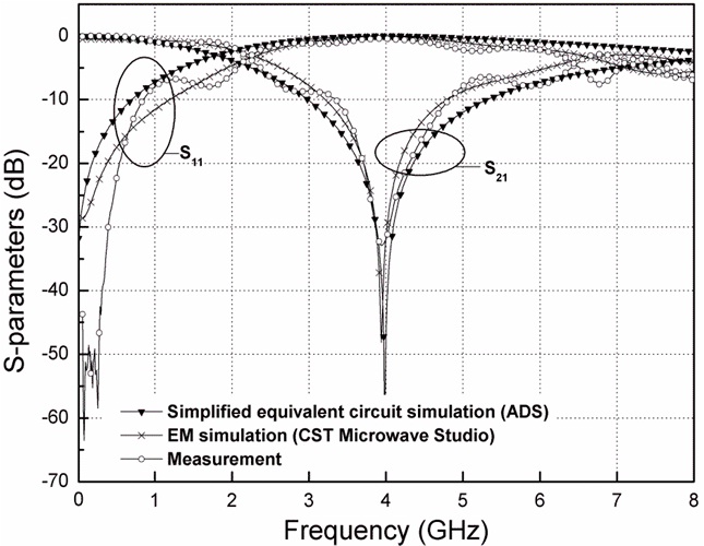
The numerical calculations are performed for the simplified equivalent circuit model (Fig. 3(c)) with the extracted parameters in Table 1 by using the ADS, and the results are compared with the results from the electromagnetic (EM) simulation using the CST Microwave Studio.
In Fig. 5, the resonance frequencies and 3dB cut-off frequencies calculated by the simplified circuit simulation and the EM simulation are plotted as functions of the radius of the etched circular pattern in the dumbbell-shaped DGS. The comparison between the results from the circuit modeling and the EM simulation shows that the proposed circuit model predicts the resonance frequencies and 3 dB cut-off frequencies with reasonable accuracy for a wide variation of radii from 2 to 10.
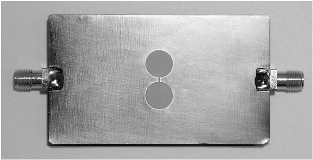
Fig. 6 illustrates the comparative transfer characteristics from the simulations and the measurement for a fabricated DGS with
This paper has presented a new equivalent circuit model of a dumbbell-shaped DGS and simple approximate expressions to extract equivalent circuit parameters. The proposed equivalent circuit model provides an improved design method and physical insight into the electromagnetic behavior of the dumbbellshaped DGS.