A dispersion analysis is performed to estimate the stopband characteristics of electromagnetic bandgap (EBG) structures with defected ground structures (DGS) of various shapes. Design guidelines are suggested for both elliptical and rectangular DGS patterns that result in a maximum stopband bandwidth for a given perforation area. This method provides a basis for numerical optimization techniques that can be used in synthesizing DGS shapes to meet bandgap requirements and layout constraints.
In high-speed printed circuit boards (PCBs), the propagation of power/ground (P/G) noise causes a significant degradation of signal integrity. Today, data rates are continuously increasing, so noise coupling through the P/G planes occurs over a wide range of frequencies. Therefore, wideband suppression of P/G noise coupling is an essential requirement for high-speed PCBs. Electromagnetic bandgap (EBG) structures have emerged as an effective solution because they have wide stopband bandwidths, high stopband attenuation, and are easily integrated with PCBs [1]. Various techniques have been proposed to improve the noise-suppression characteristics while minimizing the size of EBG structures; these include the use of high dielectric constant materials, multivia structures, cascaded EBG cells, and defected ground structures (DGSs) [1]. The employment of DGSs has a distinctive advantage over the other methods: design modifications (i.e., removing a part of a ground plane) add no cost.
In [2], circular DGS patterns are proposed for further improvement of the stopband bandwidth with a smaller perforation area. An analytical model is also presented to determine the bandgap characteristics of the proposed structure. The method proposed in the present study involves the segmentation of a transmission line with an arbitrary characteristic impedance into multiple sections so that the characteristic impedance can be regarded as a linear function of
II. OPTIMIZATION OF DGS SHAPES
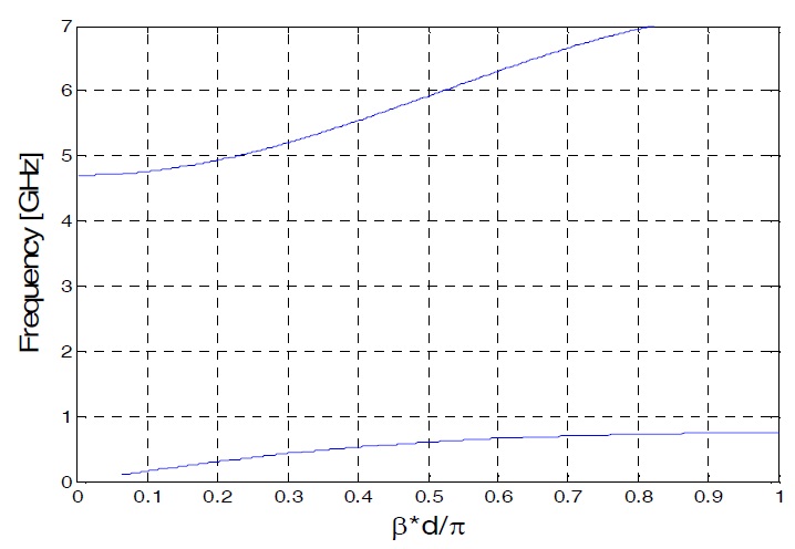
The proposed analytical method considers two lower quasi-TEM modes and estimates the start and stop bandgap frequencies (
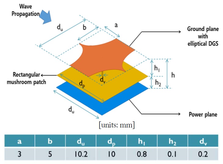
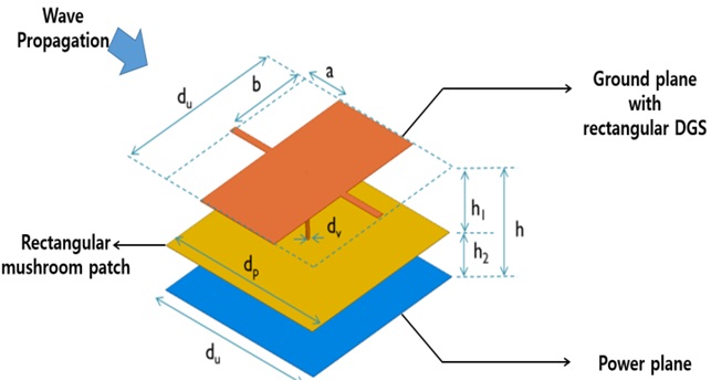
Fig. 1 shows a mushroom-type EBG structure with elliptical DGS patterns. It consists of three metal layers: a dedicated power plane (bottom), EBG patches (middle), and an elliptical DGS (top). An FR-4 substrate is used as a dielectric material (
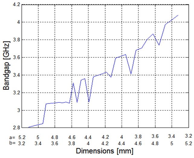
Next, the dimensions (
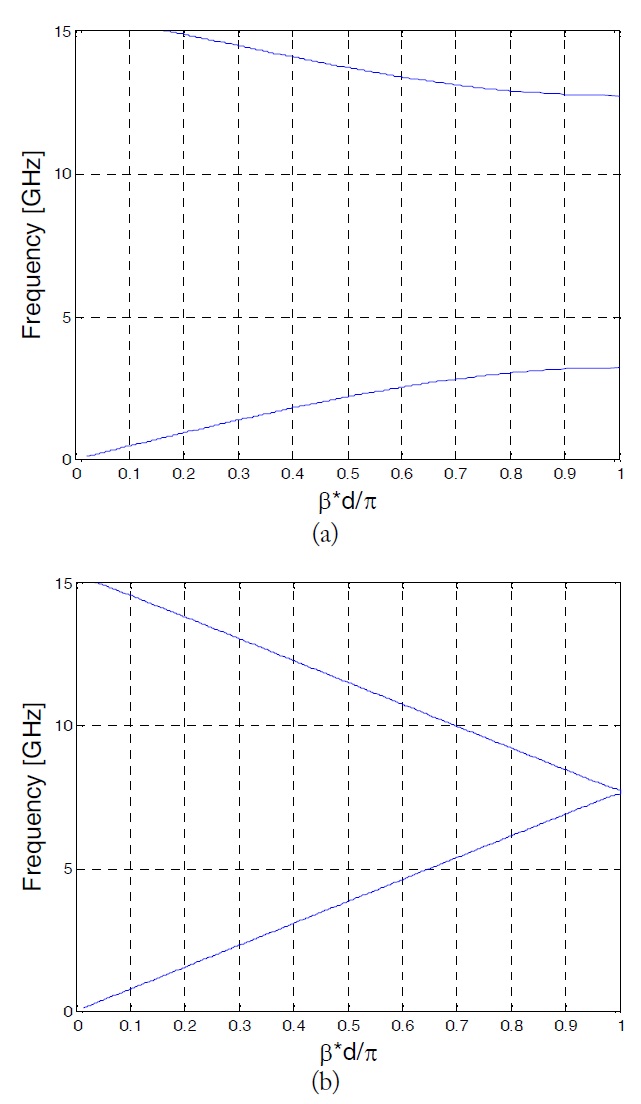
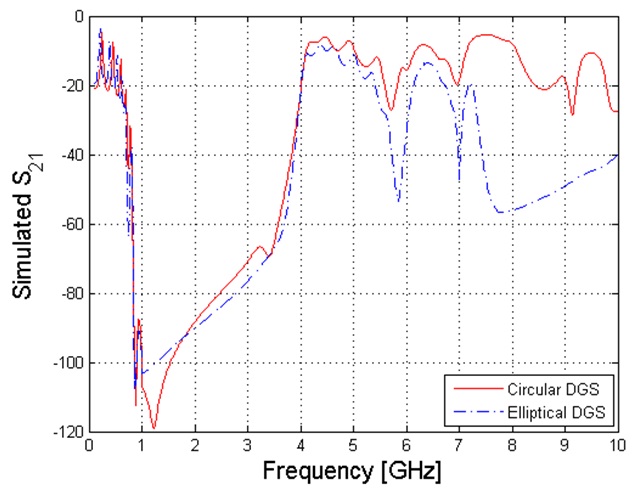
Two rectangular DGS patterns are then compared to determine whether the same principle applies to other DGS shapes, as shown in Figs. 5 and 6: one with
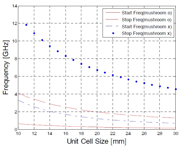
Next, we change the unit cell size (
We extend the analytical method presented in [2] to explore a variety of DGS shapes in the search for better stopband characteristics. The data presented here do not necessarily represent the optimum achievable bandgap performance for each DGS pattern; however, the analysis procedure provides a basis for numerical optimization techniques that can be used in synthesizing DGS shapes that will meet existing bandgap requirements and layout constraints.