This paper presents the equivalent circuit modelling and eigenfrequency analysis of a wideband robust capacitive radio frequency (RF) microelectromechanical system (MEMS) switch that was designed using Poly-Si and Au layer membrane for highly reliable switching operation. The circuit characterization includes the extraction of resistance, inductance, on and off state capacitance, and 𝚀-factor. The first six eigenfrequencies are analyzed using a finite element modeler, and the equivalent modes are demonstrated. The switch is optimized for millimeter wave frequencies, which indicate excellent RF performance with isolation of more than 55 dB and a low insertion loss of 0.1 dB in the V-band. The designed switch actuates at 13.2 V. The R, L, C and 𝚀-factor are simulated using Y-matrix data over a frequency sweep of 20–100 GHz. The proposed switch has various applications in satellite communication networks and can also be used for devices that will incorporate the upcoming IEEE Wi-Fi 802.11ad protocol.
In the last decade, various efforts have been made for radio frequency (RF) microelectromechanical system (MEMS) switches that are applicable to devices with switching activities that operate in RF to millimeter wave frequencies. MEMSs that are especially for RF applications have captured the interest of researchers from academia and industry. The RF MEMS has various advantages like high isolation, low insertion loss, low or near-zero power consumption, and low intermodulation distortion over their semiconductor counterparts like the field-effect transistor and p-i-n diode switches [1-5]. MEMS switches suffer from some drawbacks like low switching speed (due to mechanical deflection), high electrostatic voltage requirements of around 20–60 V for reliable switching operation, low power handling capability, reliability issues like average lifetime, fracture concerns, and packaging constraints [6-8]. RF MEMS switches incorporate a thin movable metal membrane, which actuates electrostatically for switching operations [9]. The lifetime of MEMS switches is one of the primary concerns for their use in repair-free applications like in remote places. After a few million switching cycles the metal membrane starts to suffer from fractures and this breakage usually occurs at high stress areas of the thin metal membrane.
In this paper, we present the circuit characterization and eigenfrequency analysis of a wideband robust capacitive RF MEMS switch design that incorporates a thinlayered membrane of Poly-Si and Au millimeter wave frequencies. The switch design we present is simulated using commercially available EM solvers. We present the mechanical modelling viz. stress analysis that is reported in detail in [10], and the analysis using different proportions of materials is also reported in [10]. We numerically calculate the force distribution and equivalent circuit parameters of the RF MEMS switch. The basic model is taken as reference [9], and various components like the
II. DESIGN AND PRINCIPLE OF OPERATION
The operational principle of the capacitive switch is mentioned in [11]. RF MEMS are usually actuated by the electrostatic principle [6]. For reliability and robustness of the switch, it is mandatory to design the switch with thick meanders to get an optimized range between the elastic recovery forces of metal and electrostatic voltage requirements for switching operation. The most common reliability issue in RF MEMS like stiction can be reduced, if the elastic recovery forces of the membrane are higher [12]. To overcome this issue of stiction, we have proposed a twin-layer membrane based on Gold (Au) and Polysilicon (Poly-Si). Gold has excellent electrical conductivity, but has low stress handling capabilities; in contrast, Poly- Si is a semiconductor, but has very high ultimate tensile strength to increase reliability. Gold (Au) is commonly used as a material for membrane design, but its ultimate tensile stress is 100 MPa, i.e., if the stress gradient crosses 100 MPa, the membrane can easily break from the areas under high stress. In contrast, the tensile strength of Poly- Si is 1.2 GPa [13] with a high Young’s modulus; thus using Poly-Si alone can increase the actuation voltage requirements.
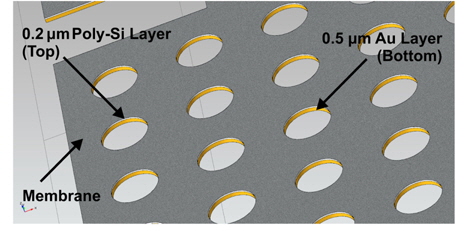
This switch incorporates a thin membrane of layered Au and Poly-Si. A layer of 0.2 μm thick Poly-Si is combined on top of a 0.5 μm thick Au layer. This combination provides high elastic recovery to reduce stiction and makes the switch more robust to handle many more switching cycles.
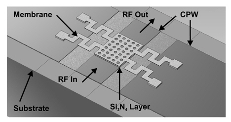
The switch is designed on quartz substrate due to its better EM wave propagation capabilities on higher frequency bands [14]. A coplanar waveguide (CPW) with wide signal line of 60 μm and 40 μm gap between the ground plane is designed over the substrate to allow or block the RF signal using thin membrane. Input and output ports of the signal line are usually coupled with coaxial cables to connect with standard RF applications. Au material is used to design the CPW due to its better stiction with silicon nitride as dielectric over the substrate. Fig. 1 shows the proposed RF MEMS switch with labeled components. When the bias voltage is provided to the electrode beneath the signal line, electrostatic force is generated, which causes vertical deflection towards the signal line. A dielectric layer of 0.2 μm thick is used between the membrane and signal line contact to change the value of the capacitance.
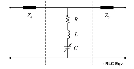
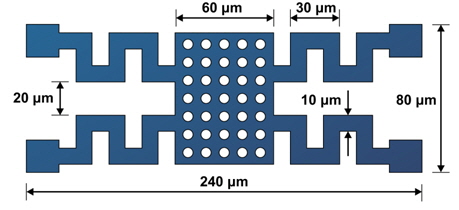
The capacitance varies either to allow the RF signal or to pass it through ground, i.e., block the RF signal. A large electrode of 80 μm × 60 μm is used for the actuation principle. The meanders help in reducing the pulldown voltage. Au is used to achieve low-voltage and Poly-Si is used for increasing robustness of the switch; hence, the best of both materials makes this switch reliable in high frequency applications. Fig. 2 demonstrates a close-up view of the membrane that shows twin layers stacked on each other. Holes are provided in the area of membrane that usually interacts with the signal line for the switching operation. Inclusion of holes in the membrane has huge advantagesit aids in attaining higher switching speeds, reduction of biaxial residual stress, reduction in air damping, and the effective mass of the membrane decreases [9]. The dimensions of the membrane are shown in Fig. 3 and the equivalent circuit model of the switch is shown in Fig. 4. The
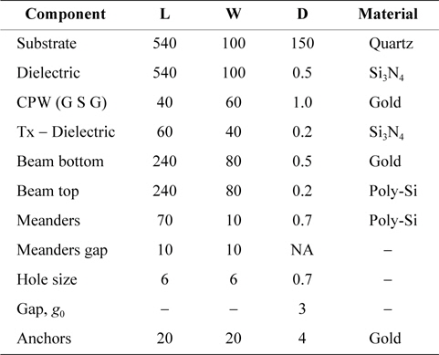
[Table 1.] Switch specifications

Switch specifications
The basic elements
[Table 2.] Extracted and fitted values
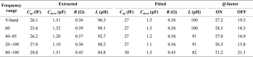
Extracted and fitted values
For the capacitive RF MEMS switch in shunt configuration between signal line and ground, the impedance

The impedance

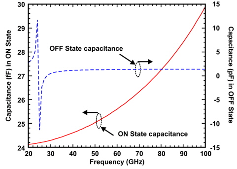
The value of the capacitance depends purely on the position of the metal membrane suspended over the signal line. The capacitance depends on the ON or OFF state of the switch. The up-state capacitance


where,
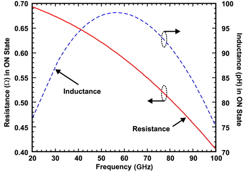
The primary factors for the calculation of the series resistance

where,
The inductance

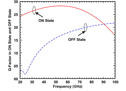
A high

where, Im (
The actuation voltage

where,
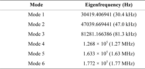
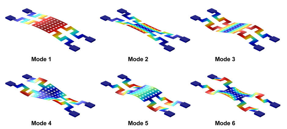
Eigenfrequency basically means the ‘characteristic’ frequency of a device or in simple words, it is the ‘ownfrequency’ of the device. It can also be thought of as the normal modes of vibrations of a system. Eigenfrequency analysis was used to find the basic modes of vibration of the RF MEMS switch [14]. The first six modes of the switch are shown in Fig. 8. These frequencies can be determined by solving the Lagrangian of the system, and then applying the canonical equation. The deflection at the natural frequency of the RF MEMS switch or the first mode can be determined from Fig. 8. The series of next frequencies are at values that are whole number multiples of the fundamental frequency. The first six eigenfrequencies are given in Table 3.
[Table 3.] Eigenfrequencies and membrane deflection

Eigenfrequencies and membrane deflection
The equation of motion of a membrane that is subjected to harmonic force is considered. The harmonic motion of the mass-spring system in a single degree of freedom is usually modelled with a differential equation of second-order as:

where,
As the membrane is composed of two materials, the spring constant

where,

The effective spring constant
The natural frequency of the membrane depends on the equivalent spring constant and the effective mass, and the natural frequency

To determine the first mode of eigenfrequency

where,
The RF performances for the device in both switching states are extracted by

where,

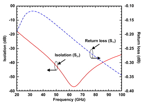
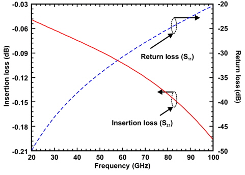
Excellent isolation above 50 dB can be achieved in the V-band and above 40 dB from 45–85 GHz. At 60 GHz, the switch results in maximum isolation of 58 dB. The results indicate 0.07 to 0.15 dB insertion loss in the ON state from 40–85 GHz. The return loss is in between 0.15–0.30 dB in the OFF state and 25–40 dB for 85 GHz and 40 GHz, respectively. The proposed switch also indicates moderate performance until 100 GHz with 35 dB of isolation and 0.2 dB insertion loss. The
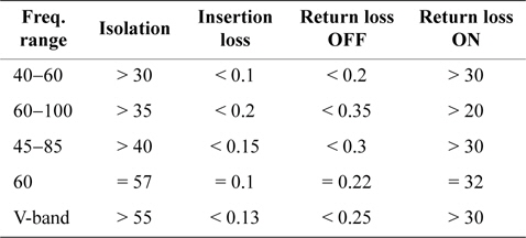
Table 4 summarises the simulated RF performance results for the switch at different frequency bands. The RF performance for 40.60 GHz, 60–100 GHz, V-band (60–75 GHz), 60 GHz, and 45–85 GHz is given in the table. The plots shown in Figs. 9 and 10 indicate the RF performance from 20–100 GHz. The typical values for RF MEMS switches that operate in millimeter wave frequencies usually result in isolation of approximately 20 dB and insertion loss having typical values of 0.3– 0.4 dB, because on moving towards the higher frequency spectrum, the performance start decreasing.
[Table 4.] RF performance analysis

RF performance analysis
A wideband robust capacitive RF MEMS switch is designed and characterized. The combined layer membrane shows excellent RF performance in millimeter wave frequencies up to 100 GHz, while requiring low actuation voltage. The switch incorporates a twin membrane approach to increase the reliability operation of the switch. The high