검색 전체 메뉴
PDF
맨 위로
OA 학술지
Fabrication of Viewing Angle Direction Brightness-Enhancement Optical Films using Surface Textured Silicon Wafers
  • 비영리 CC BY-NC
  • 비영리 CC BY-NC
ABSTRACT
Fabrication of Viewing Angle Direction Brightness-Enhancement Optical Films using Surface Textured Silicon Wafers
KEYWORD
Light-extraction optical film , KOH wet etching , LED/OLED planar lighting , (100)-oriented silicon wafer , Haze ratio
  • I. INTRODUCTION

    Recent tremendous development of LED (light emitting diode) technologies and the world-wide industrial boom has enabled the era of solid state lighting to come into our lives. One of the mainstream of LED applications is, without a doubt, solid state lighting for home, electronic goods, street lighting lamps, industry, etc. There has been very much effort for lighting applications utilizing LEDs to replace incandescent light bulbs and downlights. Although the planartype LED lighting possesses high luminance efficacy of up to ~180 lm/W (at package level cool white 4,750~7,040 K), color index, and long lifetime, there are still strict restrictions that should meet the customers’s needs, such as the avoidance of shiny glare of LED point sources and achievement of high brightness toward the viewing angle. Usually, for the application of LED lighting to the downlights and planar type lamps, uniform illuminance is critical. Therefore optical films are generally employed when LED lighting devices are assembled and packaged. Their role is to redistribute the light rays coming out from the point LED sources and uniformly radiate onto the forward direction without sacrificing illuminance [1-4].

    There have been great efforts to form upright pyramid geometry, especially in Si solar cell technologies [5-8]. Texturization of a (100) oriented mono-crystalline silicon substrate with a subsequent deposition of an anti-reflection coating has become a well-established method for the minimization of reflection losses. Anisotropic etching, such as sodium or potassium hydroxide solutions, is used to form pyramidal structures on the mono-crystalline silicon solar cell surfaces [9-11]. Elimination of light trapping by upright pyramid geometry can be attributed to the increase of the escape cone for light extraction caused by the alteration of propagation direction of light rays at the pyramid surfaces [12].

    Here, we report a quite simple and efficient way of fabricating uniform high light-extraction optical films for LED lighting by utilizing micro/nano-patterned silicon wafer masters.

    II. METHODS

    In this section, we briefly describe the fabrication method. The method for surface texturization utilizing an anisotropic etching process is well established [13, 14], but we moved a step ahead to achieve efficient and cheap ways of fabricating improved light-extracting films.

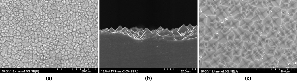
    First, master patterns were simply and efficiently fabricated by KOH additives under the proper wet etching conditions. 4” (100)-orientation silicon wafers were etched by formulated solutions (DI water : IPA : KOH = 50:47:3 wt%) along with ultrasonic vibration of 40 kHz for 50~70 minutes. Etched textures were slightly different depending on the detailed etching conditions. The surface texturing of etched wafer surfaces was shown in Fig. 1(a). Quite well shaped nano-, and micro-sized pyramid patterns were formed on the entire 4”-wafer surfaces. Orientational positions and size distributions of individual patterns were observed to be random (within a range from 100 nm to 5 μm) under the SEM observations. The apex angle of the pyramids is estimated to be 70.5°, which is fixed due to the intrinsic crystalline nature of (100)-oriented silicon wafers. We could successfully wet-etch the wafers up to 8” so far, therefore larger wafer etching can also be done.

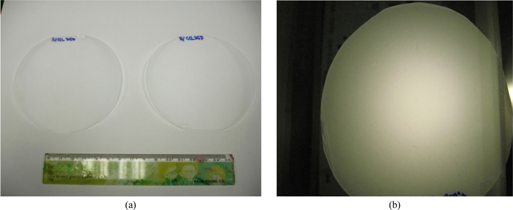
    Secondly, a replica process of patterns onto the film was carried out by coating molding fluids (film thickness ~ 10 μm) on top of Si-wafer and pressing base plates (transparent PC (polycarbonate), PMMA (poly methyl methacrylate) from i-components Inc.) followed by UV curing (UVA 360 nm, 120 W with energy 435 mJ/cm2). Using the fabricated film as a working mold (reverse pattern), replication of pattern onto a 4” film was performed again. Replication of pyramid patterns onto the films using the master mold was quite successful, and surface roughness was the same as that of master patterns by SEM image in Fig. 1(c).

    III. RESULTS & DISCUSSION

    When we put the 4” fabricated optical films on the LED lighting, we observed the transmitted light was quite uniform and hazy by naked eye so that no pointy shape of LEDs was detectable (Fig. 2). Haze was measured by using a hazemeter (NDH-5000, NIPPON DENSHOKU) for several samples made of PMMA and PC. The results were listed in Table 1. One can find that haze ratio values (= Diffuse transmittance/Total transmittance) are over 90%, which is a quite unique characteristic since high transmittance of clear PMMA or PC sheets usually results in low haze ratio.

    [TABLE 1.] Optical performance of replicated film, i.e., haze ratio (= Diffuse transmittance/Total transmittance) shows very large values over 90%

    label

    Optical performance of replicated film, i.e., haze ratio (= Diffuse transmittance/Total transmittance) shows very large values over 90%

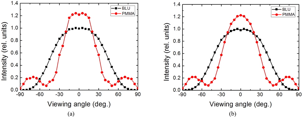
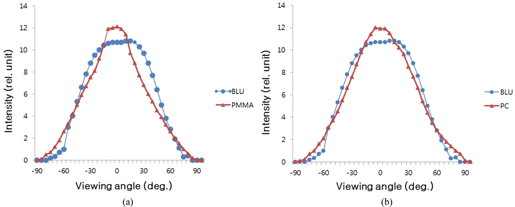
    Next, we checked the brightness enhancement effect of putting films on top of a BLU (backlight unit, white light source), from which the diffuser film was removed, by comparing it with & without (w/o) optical films. We used index-matching oil between the BLU and the optical film for the maximum brightness. Intensity profiles were measured by Goniophotometer (C-type, Pimacs). Fabricated films were attached in front of the BLU source and placed at the center of the Goniophotometer. The detector was 12 meters away from it, and intensity distributions were measured from -90 to 90 degrees at the interval of 5 degrees. The intensity of BLU w/o film shows broad illumination across the visible wavelength region. However, when optical films were employed, the maximum intensity was measured to be 13~14% at the center. Intensity profile was also dominated ~±20° along the viewing angle direction (Fig. 3), but intensity outside the viewing angle decreased as the result of light redistribution, i.e. photonic energy redistribution from the tails to the center (viewing angle) occurred as shown in Figs. 3 and 5. Compared with the previous work [1], brightness enhancement (15~20%) is lower, maybe due to dirt or imperfect index matching between film and BLU.

    We claim that the proposed fabrication process is quite unique, simple and most of all, cost-saving. There are many methods that employ conventional photo-lithography and semi-conductor fabrication processes. These techniques require high cost and many more process steps including two step-etch masking and dry etching and replications [1]. In contrast, our proposed method uses only simple wet etching along with sonication, moreover master patterns can be fabricated as large as the available silicon wafer (up to 8” in this work).

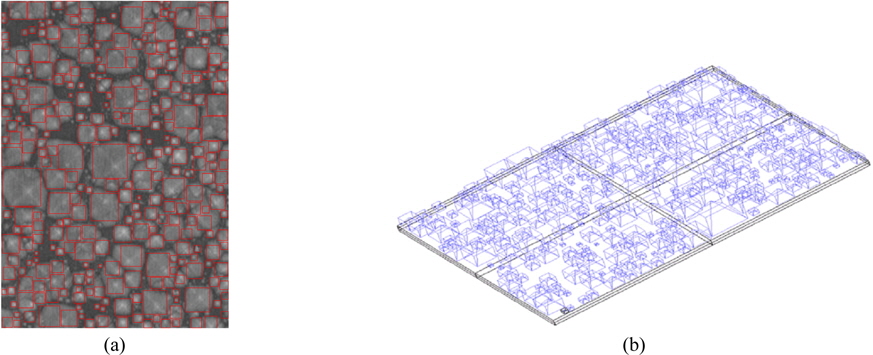
    Next, computer simulation with LightToolsTM was carried out for comparison and established simple modeling to investigate the physical nature inside. Figure 4 shows an SEM image of the surface texturing employed for the texture modeling and the texture modeled in LightToolsTM for optical simulations with wavelength of 550 nm. The simulation results presented in Fig. 5 reproduced essentially the same features observed in the measurements. The discrepancy between measured and simulated results including numerical values of viewing angle and brightness enhancement etc. can be attributed to the facts that the reflection property of the real BLU is not to be modeled as either a specular mirror or a Lambertian reflector and the reflectance of the BLU is less than 100%.

    We have already checked alternative fabrication methods for pattern master using photo-lithography and dielectric etch mask (SiO2, SiNx) to form highly ordered lattice-like patterns with uniform size [1, 2, 15]. When we compare the uniformity and brightness of films between randomlypositioned and periodic-positioned patterns, data showed no considerable differences in brightness enhancement.

    IV. CONCLUSION

    In summary, we introduced the simple fabrication method to form random-positioned and random-sized pyramid patterns on the (100) silicon wafer surface. A simple way of replication was also introduced and optical performances were measured. We could check the feasibility for LED/OLED lighting applications by simply laminating on top of LED lamps and testing uniformity and brightness and shiny glare. Fabricated optical films in this work turned out to be quite suitable for targeted LED lamps. Simulational results also turned out to be in good agreement with experimental data. Furthermore, the proposed method is quite simple, efficient and most of all cost-saving that a large area pattern master will meet the requirement of cheap mass-production.

참고문헌
  • 1. Lin L., Shia T. K., Chiu C. J. 2000 “Silicon-processed plastic micro- pyramids for brightness enhancement applications,” [J. MicroMech. MicroEng.] Vol.10 P.395-400 google cross ref
  • 2. Pettersson U., Jacobson S. 2006 [Tribology International] Vol.39 P.695-700
  • 3. Sun W., Tien T. C., Pan J., Yang T., Tsuei C., Huang Y. 2013 “Simulation and comparison of the lighting efficiency for household illumination with LEDs and fluorescent lamps,” [Journal of the Optical Society of Korea] Vol.17 P.376-383 google cross ref
  • 4. Jo B.-Y., Ko J.-H. 2013 “Analysis of color uniformity of white LED lens packages for direct-lit LCD backlight applications,” [Journal of the Optical Society of Korea] Vol.17 P.506-512 google cross ref
  • 5. Campbell P., Green M. A. 1987 “High performance light trapping textures for monocrystalline silicon solar cells,” [J. Appl. Phys.] Vol.62 P.243-249 google cross ref
  • 6. Rodriguez J. M., Tobias I., Luque A. 1997 “Random pyramidal texture modelling,” [Solar Energy Materials and Solar Cells] Vol.45 P.241-253 google cross ref
  • 7. Yagi T., Uraoka Y., Fuyuki T. 2006 “Ray-trace simulation of light trapping in silicon solar cell with texture structures,” [Solar Energy Materials and Solar Cells] Vol.90 P.2647-2656 google cross ref
  • 8. Basore P. A. 1990 “Numerical modeling of textured silicon solar cells using PC-1D,” [IEEE Tr. El. Devices] Vol.37 P.337-343 google cross ref
  • 9. Palik E. D., Glembocki O. J., Heard I., Burno P. S., Tenerz L. 1991 “Etching roughness for (100) silicon surfaces in aqueous KOH,” [J. Appl. Phys.] Vol.70 P.3291-3300 google cross ref
  • 10. Vu Q. B., Stricker D. A., Zavracky P. M. 1996 “Surface characteristics of (100) silicon anisotropically etched in aqueous KOH,” [J. Electrochem. Soc.] Vol.143 P.1372-1375 google cross ref
  • 11. Arndt R. A., Allison J. F., Haynos J. G., Meulenberg Jr. A. 1975 “Optical properties of the COMSAT non-reflective cell,” [Proc. 11th IEEE International Photovoltaic Specialists Conference] P.40-43 google
  • 12. Xi J.-Q., Luo H., Pasquale A. J., Kim J. K., Schubert E. F. 2006 “Enhanced light extraction in GaInN light-emitting diode with pyramid reflector,” [IEEE Photon. Technol. Lett.] Vol.18 P.2347-2349 google cross ref
  • 13. Verlinden P., Evrard O., Muzy E., Crahay A. 1992 “The surface texturization of solar cells: A New. Method using V-grooves with controllable sidewall,” [Energy Materials and Solar Cells] Vol.26 P.71-78 google cross ref
  • 14. King D. L., Buck M. E. 1991 “Experimental optimization of an anisotropic etching process for random texturization of silicon solar cells,” [Proc. 22nd IEEE International Photovoltaic Specialists Conference] Vol.1 P.303-308 google
  • 15. Zhu J., Yu Z., Burkard G. F., Hsu C., Connor S. T., Xu Y., Wang Q., McGehee M., Fan S., Cui Y. 2009 “Optical absorption enhancement in amorphous silicon nanowire and nanocone arrays,” [Nano Letters] Vol.9 P.279-282 google cross ref
OAK XML 통계
이미지 / 테이블
  • [ FIG. 1. ]  SEM images of the surface texturing of etched wafer surfaces, (a) top view and (b) side view. Well-formed pyramid patterns were observed. Positional and size-distribution of individual patterns look quite random, which is good to prevent any optical effects, such as diffraction, or Moire patterns. The apex angle of a pyramid is estimated to be about 70.5°. (c) Top view of replicated patterns on the optical film using working mold. Surface roughness of film agrees quite well with silicon wafer roughness.
    SEM images of the surface texturing of etched wafer surfaces, (a) top view and (b) side view. Well-formed pyramid patterns were observed. Positional and size-distribution of individual patterns look quite random, which is good to prevent any optical effects, such as diffraction, or Moire patterns. The apex angle of a pyramid is estimated to be about 70.5°. (c) Top view of replicated patterns on the optical film using working mold. Surface roughness of film agrees quite well with silicon wafer roughness.
  • [ FIG. 2. ]  (a) Appearance of UV-cured molding film (full scale of the ruler: 15 cm), and (b) transmitted light through the fabricated PC and PMMA sheets.
    (a) Appearance of UV-cured molding film (full scale of the ruler: 15 cm), and (b) transmitted light through the fabricated PC and PMMA sheets.
  • [ TABLE 1. ]  Optical performance of replicated film, i.e., haze ratio (= Diffuse transmittance/Total transmittance) shows very large values over 90%
    Optical performance of replicated film, i.e., haze ratio (= Diffuse transmittance/Total transmittance) shows very large values over 90%
  • [ FIG. 3. ]  Intensity profiles of optical films which were fabricated from pyramid patterned,and non-patterned optical films. We used an LCD BLU (white light source) with diffuser film removed and compared the intensity profiles of (a) PMMA film and (b) PC film on top of it.
    Intensity profiles of optical films which were fabricated from pyramid patterned,and non-patterned optical films. We used an LCD BLU (white light source) with diffuser film removed and compared the intensity profiles of (a) PMMA film and (b) PC film on top of it.
  • [ FIG. 5. ]  Simulation results from 550 nm in wavelength. The bottom of the BLU is assumed to be (a) a perfect (reflectance: 100%) specular mirror and (b) a perfect (reflectance: 100%) Lambertian reflector.
    Simulation results from 550 nm in wavelength. The bottom of the BLU is assumed to be (a) a perfect (reflectance: 100%) specular mirror and (b) a perfect (reflectance: 100%) Lambertian reflector.
  • [ FIG. 4. ]  (a) SEM image of the surface texturing of an etched wafer surface employed for the texture modeling and (b) the texture modeled in LightToolsTM for optical simulations.
    (a) SEM image of the surface texturing of an etched wafer surface employed for the texture modeling and (b) the texture modeled in LightToolsTM for optical simulations.
(우)06579 서울시 서초구 반포대로 201(반포동)
Tel. 02-537-6389 | Fax. 02-590-0571 | 문의 : oak2014@korea.kr
Copyright(c) National Library of Korea. All rights reserved.