검색 전체 메뉴
PDF
맨 위로
OA 학술지
Numerical Study of Polarization-Dependent Emission Properties of Localized-Surface-Plasmon-Coupled Light Emitting Diodes with Ag/SiO2 Nanoparticles
  • 비영리 CC BY-NC
  • 비영리 CC BY-NC
ABSTRACT
Numerical Study of Polarization-Dependent Emission Properties of Localized-Surface-Plasmon-Coupled Light Emitting Diodes with Ag/SiO2 Nanoparticles
KEYWORD
Light emitting diodes , Surface plasmons , Spontaneous emission , Light extraction
  • I. INTRODUCTION

    GaN based solid-state light emitting diodes (LEDs) are widely attractive as an alternative energy saving lighting device because of high efficient light emission [1, 2]. The external quantum efficiency (EQE) of light emission is given by internal quantum efficiency (IQE) and light extraction efficiency (LEE). For achieving high-efficiency LEDs, both of IQE and LEE should be high enough. The IQE is usually limited by the quality of an active medium such as an InGaN quantum well (QW), and LEE is limited by total internal reflection (TIR) in high index contrast between the semiconductor and surrounding material. Recently, the high IQE of InGaN/GaN blue LEDs was achieved with the help of rapid development of semiconductor growth technology [3, 4]. The LEE was also dramatically improved by introducing the surface patterning in both the top and bottom surfaces [5, 6]. However, in green LEDs, the IQE is still very low because of the poor crystal properties such as In dislocation and strong piezo-electric effect [7]. Moreover, in the deep UV regime, there are no transparent electrodes and encapsulation materials, leading to very poor LEE [8].

    Since pioneer work in early twenty-first century, surfaceplasmon( SP)-coupled light emitting diodes (LEDs) have been widely studied theoretically and experimentally in order to improve both IQE and LEE, especially in green LEDs [9-13]. The mechanism of IQE enhancement in SP LEDs is the resonant energy transfer from the carrier recombination in QWs to the SP mode at the metal structure, and the outcoupling of the SP mode into the radiation mode. Hence, the efficient QW-SP coupling increases the spontaneous emission (SE) rate, while the nonradiative process is reduced simultaneously. In addition, the metallic nanoparticle (NP) has very large scattering cross section to extract the light outside materials to overcome TIR. For satisfying the industrial demand, it is necessary to achieve not only the high emission efficiency but also no degradation of device performance. However, the problem in Ag NP coated LEDs is an easy oxidation of Ag which induces significant absorption of the SP mode before transition to the radiation mode. It was reported that Ag/SiO2 core-shell (CS) coated LEDs had more consistent emission efficiency than Ag NP coated LEDs [14].

    Generally, the SE rate of a dipole near a metallic structure strongly depends on the radiation direction [15]. Moreover, the emitted light from the GaN based LEDs is partially polarized according to the growth direction and the aluminum content [16-19]. Recently, researchers have paid attention to polarization of light emission in SP-coupled LEDs. Most reports are related to the Ag NP buried in the p-GaN layer, where the enhancement of the radiation power of the dipole near the Ag NP is dramatically changed by the direction of the dipole radiation [20-22]. However, the Ag NP embedded structure has several issues for the real LED device because of the irregular Ag NP size caused by the high temperature during the epitaxial process and the degradation of the crystal quality due to the Ag NPs. Moreover, there was no mention about the LEE enhancement because the structure does not include air-GaN boundary structure. One paper reported that the total photoluminescence (PL) decreases significantly by localized SP (LSP) resonant dissipation even though there is large enhancement of photoluminescence (PL) decay rate by the efficient LSP-QW coupling [23]. In this paper, we numerically study polarization dependent enhancement both of the SE rate and the LEE in a closely packed seven Ag/SiO2 CS NP coated InGaN/GaN LEDs by changing the Ag size, the thickness of SiO2, and the distance of the QWs from the surface. Finally, we suggested the optimum position of the QW in blue InGaN/GaN LEDs with Ag/SiO2 CS NPs for practical application.

    II. NUMERICAL METHODS

    Recently, the dipole radiation property near Ag NP was studied by semi-classical analysis [20, 21]. According to the reports, the SP mode could be analyzed by the theoretical model when the Ag NPs are in homogeneous media. However, it is hard to solve the optical property of Ag/SiO2 CS NP coated InGaN/GaN LEDs by the semi-classical approach because of breaking the azimuthal symmetry of the structure. In this paper, we analyze light emission properties by a full three-dimensional (3-D) finite-difference time-domain (FDTD) method [24, 25].

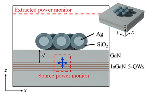
    The schematic cross section of the LED structure being considered is shown in Fig. 1. The closely packed seven identical Ag/SiO2 CS NPs lie on the p-GaN surface. The five InGaN QWs are positioned below the 70-nm-thick p-GaN layer. Each QW has the same thickness with 2 nm and the barrier between QWs is 8 nm. The refractive indices of InGaN and GaN are 2.7 and 2.46, respectively. Here, we use the perfectly matched layer (PML) absorbing boundary to realize the infinite-size space. The spatial nonuniform- grid FDTD method is used for saving the computational memory. Note that the minimum grid size is fixed as 1 nm, which is an adequate size to resolve the strongly localized field distribution in consideration of limited computational power. The dipole polarized parallel to the surface (TE-polarized dipole) or normal to the surface (TMpolarized dipole) is launched at the center of the 2-nm-thick InGaN QW. The lateral position of the dipole source is fixed at the center of the central Ag/SiO2 CS NP. The total radiation power is obtained by integrating the power flux through the monitor box surrounding the dipole source. And the extracted power is obtained by integrating the power flux through the monitor plane at 135 nm above the p-GaN surface, which corresponds around a 74-degree solid angle. The enhancement of the SE rate (γrad0rad) and the enhancement of the LEE (ηext0ext) was achieved by normalizing the total radiation power and the extracted power with those at the LED structure without Ag/SiO2 CS NPs. In all simulations, we fixed the number of Ag/SiO2 CS NPs as seven, which is the optimum condition for maximizing the extracted power [26].

    III. RESULTS AND DISCUSSION

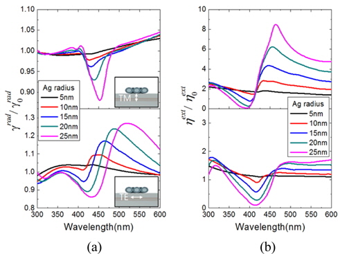
       3.1. Dependence On The Ag Size

    The LSP resonance is strongly affected by the size, the shape and the environmental materials of the metal NP [27]. Therefore, in order to improve the emission efficiency of the LEDs, the LSP resonance should be spectrally close to the emission wavelength. First, we investigated the Ag size dependence of the SE rate and the LEE with different dipole polarizations. Here, the thickness of SiO2 is fixed at 20 nm, and the source distance from the surface, d is fixed at 71 nm, the center of the first QW.

    Figure 2(a) shows γrad0rad as a function of wavelength by changing the radius of Ag. The upper graph corresponds to the TM-polarized dipole and the lower corresponds to the TE-polarized dipole. Both the TM-polarized dipole and the TE-polarized dipole have a dip near 425 nm in spectra of the SE rate. As the radius of Ag increases, the dip becomes deeper and wider with a small red-shift. This is related to the nonradiative decay rate by the Ag/SiO2 CS NPs. On the other hand, the peak is only found in the TE-polarized dipole at the longer wavelength of the dip. The origin of the enhancement of the SE rate is near-field energy coupling between the dipole emitter and the LSP mode [9-11]. We will discuss this in the next paragraph and in Sec. 3.3 in details. In Fig. 2(b), ηext0ext at different sizes of the Ag are plotted as a function of the wavelength. As the radius of Ag becomes large, it is overall enhanced in the long wavelength region at both polarizations. As the size of the Ag increases, the modal volume of the LSP resonance becomes large, so the coupling efficiency between the emitted light and the LSP mode increases. The coupled LSP mode is converted back into the radiative light. The significant reduction of the LEE is observed at a short wavelength, ~ 425 nm in both dipoles as the radius of Ag increases. This is related to the absorption of the coupled LSP mode by ohmic loss. The peak of ηext0ext in the TM-polarized dipole is more pronounced with the red-shift. This is related to the inherent radiation direction. Because the TM-polarized dipole is radiated along the in-plane direction, most of the radiated light could not escape from the GaN substrate because of TIR. Therefore, even if a small part of the light coupled to the LSP mode, the enhancement of LEE could be large. The line-shape of ηext0ext looks like the Fano-resonance, which is caused by the temporal interference between the direct radiation from the dipole and the re-radiated light from the coupled LSP mode [21, 28].

    For the further understanding of the SE rate change, we considered a simple model: a dipole emitter near a metal sphere in a homogeneous medium. This problem has an exact analytical solution based on Mie scattering theory [28-30]. The presence of the metallic NP near a dipole emitter introduces an additional nonradiative decay channel which depends only on the material property of the metal. Therefore, as the size of Ag increases, the nonradiative decay rate is enhanced, while there is no significant polarization dependence and no wavelength shift [31]. This is matched with the tendency of the dip in spectra of γrad0rad in Fig. 2(a). In contrast, when the dipole emitter is close to the metallic structure, the radiative decay rate can be also dramatically changed by the coupling effect between the dipole and the induced dipole (the so-called surface plasmon mode) according to the orientation of the dipole moment [29, 31].

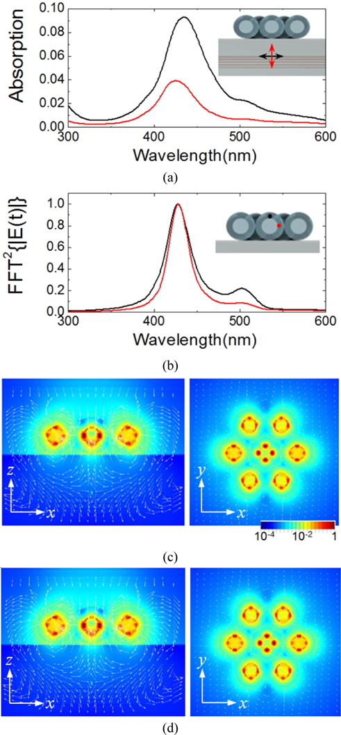
    The strength of the resonant coupling is determined by how the dipole emitter is close to the LSP mode, spatially and spectrally. We also calculated the absorption and resonance behaviors at Ag/SiO2 CS NPs in both the TM-polarized dipole and the TE-polarized dipole. Figure 3(a) shows the absorption spectra when the radius of Ag is 15 nm. The absorption spectrum is calculated by subtracting the Poynting flux from the total radiation power of the dipole source. Here, the boundary of the calculation domain with the exception of the PML layer is used as the integral surface of the Poynting flux, which should be far from a dipole source and the LSP mode at the Ag/SiO2 CS NPs. Both the TM-polarized dipole and the TE-polarized dipole have a similar absorption spectrum. The difference of the absorption intensity between the TM-polarized dipole and the TE-polarized dipole is caused by different radiation direction. Figure 3 (b) shows the LSP resonance spectra at Ag/SiO2 CS NPs when the dipole source is launched at 71 nm below the GaN surface. Note that the resonance spectrum is obtained by the discrete Fourier transform of the time-varying electric field at the maximum intensity positions after the dipole source radiation which are marked as the red dot (the left edge of the center Ag) for the TM-polarized dipole and the black dot (the top of the center Ag) for the TE-polarized dipole, as shown in the inset of Fig. 3(b). The resonance spectra look very similar to the absorption spectra. This implies that the absorption of the radiative light is caused by the ohmic loss after coupling with the LSP modes in Ag/SiO2 CS NPs. Two LSP resonance peaks are found at 428 nm, and 503 nm regardless of the dipole direction. Figure 3(c) show the cut-views of the electric field distribution of the LSP mode at 428 nm in the TM-polarized dipole. According to the xz cut-view, the electric field has a symmetric distribution along the z-axis. In addition, from the xy cut-view, the electric field near the center of Ag/SiO2 CS NP is oscillated in the radial direction. In case of the LSP resonance in the TE-polarized dipole, the direction of the electric field near the left and right Ag/SiO2 is along the x-direction shown in the left of Fig. 3 (d). Moreover, the electric field intensity near three Ag/SiO2 CS NPs on the x-axis is stronger than the intensity near the others, as shown in the xy cut-view. From these facts, the LSP resonance in the TE-polarized dipole is the coupled x-dipole modes at Ag/SiO2 CS NPs on the x-axis. In the TM resonance, the intensity at the GaN layer underneath the center Ag/SiO2 NP is stronger than that in the TE resonance. Hence, the resonant energy transfer between the QW and the LSP in the TM-polarized dipole is more efficient than in the TE-polarized dipole. We will discuss the distance dependence of γrad0rad, in Sec. 3.3.

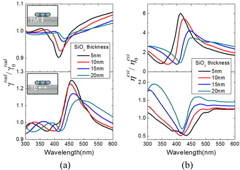
       3.2. Dependence On The SiO2-shell Thickness

    Usually, the Ag NPs are easily oxidized at the surface as time goes on. Therefore, the LSP absorption in the Ag NP is dramatically enhanced by the ohmic loss in the Ag surface [14]. In order to avoid the absorption in the Ag surface, the Ag/SiO2 CS structure was suggested for the efficient and reliable SP LED performance. However, if the SiO2 shell is too thick, γrad0rad and ηext0ext become low because of the weak coupling between the dipole emitter and the LSP mode. In addition, the resonance wavelength of the LSP mode is changed by effective index change due to the different thicknesses of the SiO2 shell [27]. In this section, we systematically investigated γrad0rad and ηext0ext with the TM-polarized and the TE-polarized dipole sources as the thickness of SiO2 is varied from 5 nm to 20 nm. In this calculation, we fixed the Ag radius at 15 nm and the source distance at 71 nm from the surface.

    Figure 4(a) shows the spectra of γrad0rad with various thicknesses of SiO2. The upper graph corresponds to the TM-polarized dipole radiation. As the thickness increases, a spectral dip is red-shifted, which is caused by increasing effective index [27]. And also, the distance from the dipole source to the Ag increases, so the nonradiative decay rate by the Ag is reduced and the resonant energy transfer between the dipole emitter and the LSP mode becomes weak. Hence, as the SiO2 shell thickens, the γrad0rad curve becomes flatter. Similarly, for the TE-polarized dipole source (shown in the lower graph of Fig. 4(a)), as the thickness of SiO2 increases, the peak is red-shifted and decreases. We also investigated the dependence of the LEE on SiO2 shell thickness with different polarizations of the dipole source. The upper graph in Fig. 4(b) corresponds to ηext0ext in the TM-polarized dipole source. As the SiO2 shell becomes thick, the enhancement of the LEE decreases due to the weak scattering at the LSP mode, and the peak wavelength is red-shifted owing to increasing effective index. In contrast, in the TE-polarized dipole, as the thicker SiO2, the more light is extracted from the GaN as shown in the lower graph of Fig. 4(b). The TE-polarized dipole has a large vertical radiation component, so Ag/SiO2 CS NPs act as strong scatterers. Therefore, in a 5-nm thickness, the LEE decreases significantly. As the SiO2 shell becomes thick, the separation distance between the Ag cores increases, hence, the scattering of the emitted light is reduced. Moreover, the thick SiO2 shell helps to enhance the light extraction because of the increase in the critical angle by inserting a middle-index layer between high-index material and low-index material.

       3.3. Dependence On The Quantum-well Position

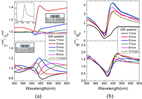
    The most important parameter for the efficient QW-SP coupling is the distance from the metallic NPs to the emitter [10, 30-31]. If the dipole emitter is close to the NPs, the quantum efficiency increases because of the stronger QW-SP coupling and light scattering. However, if the dipole emitter is very close, about a few nm, the quantum yield decreases rapidly, hence the quantum efficiency decreases by the quenching effect [28, 31]. In this section, we systematically studied the dependence of the quantum efficiency on the distance between QWs and Ag/SiO2 CS NPs according to the dipole direction. Here, we fixed the radius of Ag and the thickness of SiO2 as 15 nm and 20 nm, respectively.

    Figure 5(a) shows the dependence of γrad0rad on the distance, d, from the GaN surface to the dipole emitter. In case of the TM-polarized dipole shown in the upper graph at Fig. 5(a), γrad0rad is dramatically enhanced at all wavelengths as d decreases, especially, γrad0rad ~7 near the LSP resonance for d = 11 nm. This high enhancement is owing to the strong coupling between the dipole and the LSP mode. However, as d increases, γrad0rad goes to unity quickly. On the other hand, the SE rate in the TE-polarized dipole decreases at all wavelengths at d = 11 nm, as shown in the lower graph at Fig. 5(a). As d increases, γrad0rad goes to unity with some fluctuation in wavelength.

    This phenomenon could be understood by using the electrostatic image theory [28, 33]. According to the method of image charges, the image dipole moment, pi ~ po × (r/d)3, where po is the source dipole moment, r is the radius of the metal sphere, and d is the distance from the center of the metal sphere to the position of a dipole source. In the TM-polarized dipole, the direction of the dipole oscillation is perpendicular to the metallic surface, therefore, the induced dipole has the same direction as that of the source. Hence, as d is very small, the radiative decay rate increases dramatically. However, as d increases, the induced dipole becomes weak quickly, so the SE rate approaches to that in the bulk GaN. This analysis agrees well with the intensity distribution of LSP resonance shown in Fig. 3(c). In the case of the TE-polarized dipole, the direction of the dipole oscillation is parallel to the metallic surface, and the induced dipole has the opposite direction to the source dipole. Therefore, if the source dipole is close to the metal sphere, two dipoles are cancelled out, and its radiation efficiency is reduced. However, as d increases, the SE rate is changed by the interference effect between the source dipole and the induced dipole.

    Figure 5(b) shows the dependence of ηext0ext on the distance as a function of wavelength for the TM-polarized dipole (the upper graph) and the TE-polarized light (the lower graph). For both polarizations, as d increases, ηext0ext increases near the LSP resonance (~425 nm), which is related with reduction of the absorption by decreasing the coupling efficiency between the emitted light and the LSP mode. As we mentioned above, the Fano-line shape near the LSP resonance is owing to the temporal interference between the direct radiation from the dipole and scattered light to the LSP mode [28]. At d = 11 nm, the LEE in the TM-polarized dipole is significantly suppressed. However, as d increases, ηext0ext is dramatically enhanced and then decreases. This is originated from interplay between the re-radiation of the coupled LSP mode and the absorption by ohmic loss. As the dipole is far from the metal NPs, the light scattering to the LSP mode decreases, and the ohmic loss is reduced. Therefore, there is an optimum distance to maximize the LEE. In the case of the TE-polarized dipole, we observed two-fold enhancement of the LEE near 475 nm at d = 11 nm. This is due to the strong coupling of the emitted light with the LSP mode. As d increases, ηext0ext decreases, and then increases at d > 71 nm.

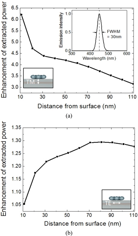
    According to these results, as d increases, the trend of the SE rate change is opposite to that of the LEE variation in both TM- and TE-polarized dipoles. For the practical application of the blue LED (λ = 450 nm ± 15nm), we calculated the enhancement of the total extracted power as a function of d as shown in Fig. 6. First, in the TM-polarized dipole, the total extracted power dramatically increases at d = 11 nm because of the great enhancement of the SE rate by strong coupling between the dipole and the LSP mode. As d increases, γrad0rad goes to unity quickly. On the contrary, ηext0ext increases until d = 71 nm, and then decreases with further increasing d. Hence, the enhancement of the total extracted power gradually decreases. On the other hand, in the TE-polarized dipole, the total extracted power is maximized about 1.3 times higher than that in the blue LED without Ag/SiO2 CS NPs at ~80 nm of the QW from the surface. The overall enhancement of the total extracted power in the TM-polarized is much higher than in the TE-polarized dipole. However, because it is very hard to extract the TM-polarized light due to its inherent radiation direction, the absolute extracted power is still much smaller than that in the TE-polarized light.

    IV. CONCLUSION

    We numerically investigated polarization-dependent SE rate and LEE in LSP-coupled LEDs. The closely packed seven Ag/SiO2 CS NPs lie on top of the GaN surface for LSP coupling with a radiated dipole. According to the dipole direction, both the SE rate and the LEE are significantly modified by LSP effect at Ag/SiO2 CS NPs when the size of Ag, the thickness of SiO2, and the position of the dipole source are varied. In the dipole oscillating parallel to the surface, the SE rate is modified by strong near-field energy coupling and the interference effect between a real dipole and an induced dipole at the Ag, and the LEE is changed due to light scattering and ohmic loss at Ag/SiO2 CS NPs. In the dipole oscillating normal to the surface, the SE rate is dramatically enhanced by extremely strong near-field coupling only when the dipole is near the Ag. And the LEE is significantly enhanced because the light mostly guided in the substrate is extracted by scattering with LSP modes. Finally we suggested the optimum QW position for maximizing extracted power in blue InGaN/GaN LEDs at each dipole direction. In TM polarization, the extracted power keeps increasing as the QW is close to the Ag/SiO2 CS NPs. However, in TE polarization, the extracted power is maximized about 1.3 times higher than that in the blue LED without Ag/SiO2 CS NPs when the QW is near 80 nm from the surface. We believe that these results help to optimize the nitride-based LSP-LED structures with different growth directions.

참고문헌
  • 1. Schubert E. F. 2006 Light-Emitting Diodes google
  • 2. Crawford M. H. 2009 “LEDs for solid-state lighting: Performance challenges and recent advances,” [IEEE J. Select. Topics Quantum Electron.] Vol.15 P.1028-1040 google cross ref
  • 3. Feezell D. F., Speck J. S., DenBaars S. P., Nakamura S. 2013 “Semipolar (20 21) InGaN/GaN light-emitting diodes for high-efficiency solid-state lighting,” [J. Disp. Technol.] Vol.9 P.190-198 google cross ref
  • 4. Cich M. J., Aldaz R. I., Chakraborty A., David A., Grundmann M. J., Tyagi A., Zhang M., Steranka F. M., Krames M. R. 2012 “Bulk GaN based violet light-emitting diodes with high efficiency at very high current density,” [Appl. Phys. Lett.] Vol.101 P.223509 google cross ref
  • 5. Wierer J. J., David A., Megens M. M. 2009 “III-nitride photonic-crystal light-emitting diodes with high extraction efficiency,” [Nat. Photon.] Vol.3 P.163-169 google cross ref
  • 6. Lee T.-X., Gao K.-F., Chien W.-T., Sun C.-C. 2007 “Light extraction analysis of GaN-based light-emitting diodes with surface texture and/or patterned substrate,” [Opt. Express] Vol.15 P.6670-6676 google cross ref
  • 7. Schwarz U. T., Braun H., Kojima K., Kawakami Y., Nagahama S., Mukai T. 2007 “Interplay of built-in potential and piezoelectric field on carrier recombination in green light emitting InGaN quantum wells,” [Appl. Phys. Lett.] Vol.91 P.123503 google cross ref
  • 8. Khan A., Balakrishnan K., Katona T. 2008 “Ultraviolet light-emitting diodes based on group three nitrides,” [Nat. Photon.] Vol.2 P.77-84 google cross ref
  • 9. Vuckovic J., Loncar M., Scherer A. 2000 “Surface plasmon enhanced light-emitting diode,” [IEEE J. Quantum Electron.] Vol.36 P.1131-1144 google cross ref
  • 10. Okamoto K., Niki I., Shvartser A., Narukawa Y., Mukai T., Scherer A. 2004 “Surface-plasmon-enhanced light emitters based on InGaN quantum wells,” [Nat. Mater.] Vol.3 P.601-605 google cross ref
  • 11. Okamoto K., Niki I., Scherer A., Narukawa Y., Mukai T., Kawakami Y. 2005 “Surface plasmon enhanced spontaneous emission rate of InGaN/GaN quantum wells probed by time-resolved photoluminescence spectroscopy,” [Appl. Phys. Lett.] Vol.87 P.071102 google cross ref
  • 12. Kwon M. K., Kim J. Y., Kim B. H., Park I. K., Cho C. Y., Byeon C. C., Park S. J. 2008 “Surface-plasmon-enhanced light-emitting diodes,” [Adv. Mater.] Vol.20 P.1253-1257 google cross ref
  • 13. Lu C.-H., Lan C.-C., Lai Y.-L., Li Y.-L., Liu C.-P. 2011 “Enhancement of green emission from InGaN/GaN multiple quantum wells via coupling to surface plasmons in a twodimensional silver array,” [Adv. Funct. Mater.] Vol.21 P.4719-4723 google cross ref
  • 14. Jang L.-W., Jeon D.-W., Kim M., Jeon J.-W., Polyakov A. Y., Ju J.-W., Lee S.-J., Baek J.-H., Yang J.-K., Lee I.-H. 2012 “Investigation of optical and structural stability of localized surface plasmon mediated light-emitting diodes by Ag and Ag/SiO2 nanoparticles,” [Adv. Func. Mater.] Vol.22 P.2728-2734 google cross ref
  • 15. Xu Y., Vuckovic J., Lee R., Painter O., Scherer A., Yariv A. 1999 “Finite-difference time-domain calculation of spontaneous emission lifetime in a microcavity,” [J. Opt. Soc. Am. B] Vol.16 P.465-474 google cross ref
  • 16. Gardner N. F., Kim J. C., Wierer J. J., Shen Y. C., Krames M. R. 2005 “Polarization anisotropy in the electroluminescence of m-plane InGaN-GaN multiple-quantum-well light-emitting diodes,” [Appl. Phys. Lett.] Vol.86 P.111101 google cross ref
  • 17. Masui H., Baker T. J., Iza M., Zhong H., Nakamura S., DenBaars S. P. 2006 “Light-polarization characteristics of electroluminescence from InGaN/GaN light-emitting diodes prepared on (11 2 2)-plane GaN,” [J. Appl. Phys.] Vol.100 P.113109 google cross ref
  • 18. Schubert M. F., Chhajed S., Kim J. K., Schubert E. F. 2007 “Polarization of light emission by 460 nm GaInN/GaN light-emitting diodes grown on (0001) oriented sapphire substrates,” [Appl. Phys. Lett.] Vol.91 P.051117 google cross ref
  • 19. Kolbe T., Knauer A., Chua C., Yang Z., Einfeldt S., Vogt P., Johnson N. M., Weyers M., Kneissl M. 2010 “Optical polarization characteristics of ultraviolet (In)(Al)GaN multiple quantum well light emitting diodes,” [Appl. Phys. Lett.] Vol.97 P.171105 google cross ref
  • 20. Kuo Y., Ting S. Y., Liao C. H., Huang J. J., Chen C. Y., Hsieh C., Lu Y. C., Chen C. Y., Shen K. C., Lu C. F., Yeh D. M., Wang J. Y., Chuang W. H., Kiang Y. W., Yang C. C. 2011 “Surface plasmon coupling with radiating dipole for enhancing the emission efficiency of a light-emitting diode,” [Opt. Express] Vol.19 P.A914-A929 google cross ref
  • 21. Kuo Y., Chang W. Y., Chen H. S., Kiang Y. W., Yang C. C. 2013 “Surface plasmon coupling with a radiating dipole near an Ag nanoparticle embedded in GaN,” [Appl. Phys. Lett.] Vol.102 P.161103 google cross ref
  • 22. Kuo Y., Chang W. Y., Chen H. S., Wu Y. R., Yang C. C., Kiang Y. W. 2013 “Surface-plasmon-coupled emission enhancement of a quantum well with a metal nanoparticle embedded in a light-emitting diode,” [J. Opt. Soc. Am. B] Vol.30 P.2599-2606 google cross ref
  • 23. Jiang S., Hu Z., Chen Z., Fu X., Jiang X., Jiao Q., Yu T., Zhang G. 2013 “Resonant absorption and scattering suppression of localized surface plasmons in Ag particles on green LED,” [Opt. Express] Vol.21 P.12100-12110 google cross ref
  • 24. Taflove A., Hagness S. 2000 Computational Electrodynamics: The Finite-Difference Time-Domain Method google
  • 25. 0000 Lumerical Solutions, Inc. - Innovative Photonic Design Tools google
  • 26. Moon S.-K., Yang J.-K. 2014 “Effect of number of Ag/SiO2 core-shells on quantum efficiency of InGaN/GaN light emitting diodes,” google
  • 27. Kelly K. L., Coronado E., Zhao L. L., Schatz G. C. 2003 “The optical properties of metal nanoparticles: The influence of size, shape, and dielectric environment,” [J. Phys. Chem. B] Vol.107 P.668-677 google
  • 28. Mertens H., Koenderink A. F., Polman A. 2007 “Plasmonenhanced luminescence near noble-metal nanospheres: Comparison of exact theory and an improved Gersten and Nitzan model,” [Phys. Rev. B] Vol.76 P.115-123 google
  • 29. Kim Y. S., Leung P. T., George T. F. 1988 “Classical decay rates for molecules in the presence of a spherical surface: a complete treatment,” [Surf. Sci.] Vol.195 P.1-14 google cross ref
  • 30. Colas des Francs G., Bouhelier A., Finot E., Weeber J. C., Dereux A., Girard C., Dujardin E. 2008 “Fluorescence relaxation in the near?field of a mesoscopic metallic particle: Distance dependence and role of plasmon modes,” [Opt. Express] Vol.16 P.17654-17666 google cross ref
  • 31. Novotny L. 2007 “Spectral dependence of single molecule fluorescence enhancement,” [Opt. Express] Vol.15 P.14266-14274 google cross ref
  • 32. Abram I., Rovert I., Kuszelwicz R. 1998 “Spontaneous emission control in semiconductor microcavities with metallic or Bragg mirrors,” [IEEE J. Quantum Electron.] Vol.34 P.71-76 google cross ref
  • 33. Zhang Z., Lim D., Diaz R. E. 2013 “Image theory for plasmon-modified luminescence near nanospheres,” [Proc. SPIE] Vol.8595 P.859508 google
OAK XML 통계
이미지 / 테이블
  • [ FIG. 1. ]  Schematic cross section of Ag/SiO2 CS NPs on InGaN/GaN LEDs.
    Schematic cross section of Ag/SiO2 CS NPs on InGaN/GaN LEDs.
  • [ FIG. 2. ]  Dependence of (a) γrad/γ0rad and (b) ηext/η0ext on the radius of Ag cores at Ag/SiO2 CS coated InGaN/GaN LED structure. The upper graphs are for the TM-polarized dipole and the lower graphs are for the TE-polarized dipole. All spectral results are normalized by the results at the LED structure without the Ag/SiO2 CS NPs.
    Dependence of (a) γrad/γ0rad and (b) ηext/η0ext on the radius of Ag cores at Ag/SiO2 CS coated InGaN/GaN LED structure. The upper graphs are for the TM-polarized dipole and the lower graphs are for the TE-polarized dipole. All spectral results are normalized by the results at the LED structure without the Ag/SiO2 CS NPs.
  • [ FIG. 3. ]  LSP absorption and resonance behavior at seven Ag/SiO2 CS NPs on the GaN surface. (a) Absorption spectra (b) Resonance spectra (c) Electric field distribution at the resonance, λ = 428 nm in the TM-polarized dipole excitation. The left is the xz cut-view of electric field. The right is the xy cut-view of the electric field. (d) Electric field distribution at the resonance, λ = 428 nm in the TE-polarized dipole excitation. The arrows in (c) and (d) indicate the direction of the electric field.
    LSP absorption and resonance behavior at seven Ag/SiO2 CS NPs on the GaN surface. (a) Absorption spectra (b) Resonance spectra (c) Electric field distribution at the resonance, λ = 428 nm in the TM-polarized dipole excitation. The left is the xz cut-view of electric field. The right is the xy cut-view of the electric field. (d) Electric field distribution at the resonance, λ = 428 nm in the TE-polarized dipole excitation. The arrows in (c) and (d) indicate the direction of the electric field.
  • [ FIG. 4. ]  Dependence of (a) γrad/γ0rad and (b) ηext/η0ext on the SiO2-shell thickness at Ag/SiO2 CS coated InGaN/GaN LED structure. The upper graphs are for the TM-polarized dipole and the lower graphs are for the TE-polarized dipole.
    Dependence of (a) γrad/γ0rad and (b) ηext/η0ext on the SiO2-shell thickness at Ag/SiO2 CS coated InGaN/GaN LED structure. The upper graphs are for the TM-polarized dipole and the lower graphs are for the TE-polarized dipole.
  • [ FIG. 5. ]  Dependence of (a) γrad/γ0rad and (b) ηext/η0ext on QW position at Ag/SiO2 CS NP coated InGaN/GaN LED structure. The upper graphs are for the TM-polarized dipole and the lower graphs are for the TE-polarized dipole.
    Dependence of (a) γrad/γ0rad and (b) ηext/η0ext on QW position at Ag/SiO2 CS NP coated InGaN/GaN LED structure. The upper graphs are for the TM-polarized dipole and the lower graphs are for the TE-polarized dipole.
  • [ FIG. 6. ]  The enhancement of extracted power as a function of the QW distance from the top surface of Ag/SiO2 CS coated InGaN/GaN blue LEDs at (a) TM-polarized dipole and (b) TE-polarized dipole. The inset graph at (a) indicates the spectrum of a reference LED.
    The enhancement of extracted power as a function of the QW distance from the top surface of Ag/SiO2 CS coated InGaN/GaN blue LEDs at (a) TM-polarized dipole and (b) TE-polarized dipole. The inset graph at (a) indicates the spectrum of a reference LED.
(우)06579 서울시 서초구 반포대로 201(반포동)
Tel. 02-537-6389 | Fax. 02-590-0571 | 문의 : oak2014@korea.kr
Copyright(c) National Library of Korea. All rights reserved.