Pb(Zr0.52Ti0.48)O3 thin films of 1.5 μm thickness were grown on Pt/Ti/Gd3Ga5O12 substrate by RF magnetron sputtering at annealing temperatures ranging from 550℃ to 700℃. We evaluated the residual stress, by using a William-Hall plot, as a function of the annealing temperatures of PZT thin film with a constant thickness. As a result, the residual stresses of PZT thin film of 1.5 μm thickness were changed by varying the annealing temperature. Also, we measured the hysteresis characteristic of PZT thin films of 1.5 μm thickness to evaluate for application of an optoelectronic device.
Recently, the use of an optoelectronic device as a light modulator has been the subject of intensive research [1,2]. In particular, magneto-optic spatial light modulators (MOSLMs), which consist of an upper electrode, lead zirconate titanate (Pb(ZrxTi1- x)O3, (PZT)) thin film, a bottom electrode, a magnetic optic layer (garnet film) and a substrate, have been given particular attention due to the high switching speed of about 15 nanoseconds. In the device, PZT thin film stresses the magnetic optic layer when applying a voltage to the PZT thin film, and magnetization switching in the magnetic optic layer is simultaneously induced. The PZT thin film, in the MOSLM device, has been widely used over the past few decades in actuator, memory, and sensor devices due to its low coercive field, high remnant polarization, high dielectric constant and high Curie temperature. Therefore, much research has been conducted on various substrates for a range of applications [3,4].
However, PZT thin film has limitations, whereby the evaporation of Pb during the manufacturing process causes inhomogeneity in the composition of the PZT thin film and cracks on the PZT thin film can be generated by the mismatch of thermal expansion coefficient between the PZT thin film and the substrate. Therefore, the suppression of the compositional change and the cracks in growing PZT thin film on a substrate needs to be considered. In general, MOSLM devices use Gd3Ga5O12 (SGGG) substrates because the SGGG substrate has a similar thermal expansion coefficient (TEC), 9.2×10⁻⁶/K [5], as that of PZT thin film, 7.0×10⁻⁶/K [6]. In the case of growing PZT thin film on an SGGG substrate, we can expect residual tensile stress and surface cracking due to the structural mismatch and thermal mismatch between the PZT thin film and SGGG substrate.
In this paper, we fabricated PZT thin film on Pt/Ti/glass and SGGG substrates using the sputtering method. In addition, we investigated the structural property of PZT thin film as a function of annealing temperature.
[Table 1.] Sputtering conditions of PZT thin film.
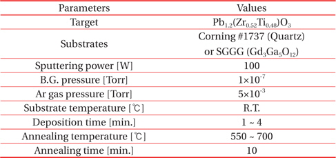
Sputtering conditions of PZT thin film.
PZT thin films were deposited onto a Corning #1737 (Quartz) or (110) SGGG substrate by RF magnetron sputtering with an Ar pressure of 0.4Pa. The Pb1.2(Zr0.52Ti0.48)O3 target with a morphotrophic composition of Zr/Ti = 52/48 was used for PZT thin film deposition to compensate Pb evaporation for the evaporation and annealing process. The structures using Pt/Ti/#1737 or SGGG in this paper were composed of a Pt bottom electrode (thickness 300 nm), a Ti layer (thickness 10 nm), and #1737 or SGGG substrates (0.5 mm thickness), namely a Pt/Ti/#1737 or (110) SGGG substrate. The deposition of the PZT thin film on the two types of substrates was performed under an RF power of 100W. In order to evaluate the dependence of PZT thin film on the annealing temperature, we conducted annealing of the deposited PZT films at temperatures ranging from 550 to 700℃ for 10minutes in an electric furnace.
The microstructure of the deposited PZT thin films was observed using a microscope and SEM, and the crystalline structure was measured using an X-ray diffractometer (XRD). From XRD data, the residual stress of the PZT thin film deposited at different annealing temperatures was calculated using a William and Hall curve. The P-E hysteresis curves of films with different thicknesses were investigated using a Sawyer-Tower circuit. The displacement property of the specimen was measured using Laser displacement analysis.
3.1 SEM comparison of PZT thin films deposited on different substrates
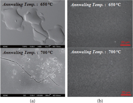
Figure 1 shows the SEM surface morphology of PZT thin films deposited on Corning #1737 (Quartz) and SGGG substrates at annealing temperatures of 650℃ and 700℃, respectively. As shown in Fig. 1, the PZT thin films on the Corning #1737 substrate showed delamination from the substrate and cracking on the PZT film, regardless of annealing temperatures. However, the PZT thin films on the SGGG substrate did not show delamination and cracking on the PZT film, despite the variation of annealing temperatures. This can be explained by the difference of thermal expansion coefficient between the Corning #1737 (Quartz) substrate of 0.3×10⁻⁶/K, the SGGG substrate of 9.2×10⁻⁶/K, and the PZT thin films of 7.0×10⁻⁶/K. Therefore, SGGG substrate can be used for growing PZT thin film without defects.
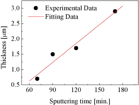
Figure 2 shows the thickness variation of PZT thin film on SGGG substrate as a function of sputtering time at room temperature. The figure shows that the thickness of the PZT thin film is proportional to sputtering time.
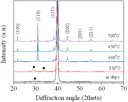
Figure 3 shows the XRD patterns of PZT thin films deposited on Pt/Ti/SGGG substrate as a function of annealing tempera- tures. Figure 3 shows that the reflection from the Pb dominated pyrochlore peak (expressed as a solid rectangle) present in the as-deposited PZT thin film and the PZT thin film annealed at 550℃ due to the excess of Pb. However, the PZT film on SGGG annealed at temperatures ranging from 600℃ to 700℃ showed pure perovskite PZT peaks. These results show that the crystalline phase of PZT film on Pt/Ti/SGGG substrate can be greatly affected by annealing temperature. When the annealing temperature was increased from 550℃ to 700℃, the intensity of the perovskite PZT peak was greatly increased, as shown in Fig. 3.
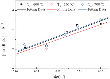
Figure 4 shows the relationship between βcosθ/λ and sinθ/λ, using a William and Hall curve [7], to investigate the stress of the deposited PZT films with different annealing temperatures, obtained from the FWHM of XRD data.

where, β : FWHM [radian]θ : Peak valuesλ : Wavelength of X-rayε : Average grain sizeη : Average stress of films
From this plot, we can evaluate the stress of the PZT thin films on SGGG by calculating the gradient of lines. The stress values, η, of the PZT thin films on SGGG annealed at 600℃, 650℃ and 700℃ were 0.01632, 0.01534 and 0.01630, respectively. This means that the PZT thin film deposited at 650℃ has the lowest stress in this annealing condition. In particular, the stress value, η, of the PZT thin film annealed at 700℃ increased compared with that of PZT thin film deposited at 650℃. It can be considered that the fluctuation of the composition in the PZT thin film occurred due to high annealing temperature, as reported by Aoki [8].
3.3 Polarization vs electric field
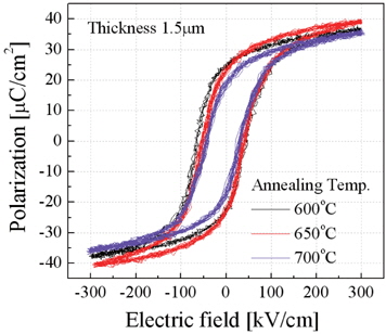
The polarization vs electric field (P-E) curves obtained by various annealing temperatures are shown in Fig. 5. As shown in Fig. 5, the saturation of hysteresis loops occurred in all PZT thin films on SGGG substrate, regardless of annealing temperature.
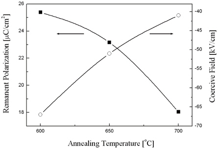
Figure 6 shows the remanent polarization (Pr) and coercive field (Ec) of PZT thin films on SGGG as a function of annealing temperature. When the annealing temperature was increased from 600 to 700℃, the remanent polarization (Pr) values of PZT thin films decreased from 25.38 μC/cm2 to 18.04 μC/cm2. Also, the coercive field (Ec) values of PZT thin films increased with annealing temperatures. It is well known that a device with high remanent polarization and low coercive field has an advantage in application for a high speed memory device due to a low switching energy [9].
We investigated the dependence of annealing temperature on the characteristics of PZT thin film (1.5 μm) on Pt (300 nm) / Ti(10 nm) / Corning #1737 (Quartz) or Gd3Ga5O12 substrates by RF magnetron sputtering. The PZT thin film on Gd3Ga5O12 substrates, annealed at 650℃, showed no crack and the lowest residual stress, η of 0.01632. Also, The PZT thin film showed the characteristics of high remanent polarization and low coercive field. Therefore, the PZT thin film on Gd3Ga5O12 substrates, annealed at 650℃, can be applicable for use in a magneto-optic spatial light modulator and high speed memory device.