검색 전체 메뉴
PDF
맨 위로
OA 학술지
Similarity Analysis for the Dispersion of Spiraling Modes on Metallic Nanowire to a Planar Thin Metal Layer
  • 비영리 CC BY-NC
  • 비영리 CC BY-NC
ABSTRACT
Similarity Analysis for the Dispersion of Spiraling Modes on Metallic Nanowire to a Planar Thin Metal Layer
KEYWORD
Silver nanowire , Planar insulator-metal-insulator geometry
  • I. INTRODUCTION

    In realizing integrated nanophotonic circuits, a promising key is the use of surface plasmons, collective electron oscillations that allow the localization, confinement, and transmission of electromagnetic energy [1, 4]. Various geometries for plasmonic waveguides and integrated components have been suggested; these include grooves and slots in metal films [2-5], metal strips [6-8], dielectric strips deposited on a metal film [9], metal caps on a silicon-on-insulator rib waveguide [10-12], and others [13-15].

    An alternative approach to achieve integrated nanophotonic circuits involves utilizing the nanowire (NW)-based plasmonic waveguides, which are typical one-dimensional waveguide structures with relatively low losses in visible and near-infrared spectral ranges [16-20]. To understand the properties of NW-based waveguides, it is essential to investigate their modal dispersion behavior. Schmidt and Russell established a connection between the dispersion of propagating modes on NW geometry and the dispersion of those on planar metal-insulator geometry with a single interface [17]. For an NW radius less than 100 nm, however, there is wide discrepancy owing to interaction with the electromagnetic field.

    In this study, we propose a simple model to elucidate the dispersion behavior of spiraling modes on silver nanowire by building a relationship with the planar insulator-metal- insulator geometry. This approximated analysis is compared with a more exact solution obtained by solving Maxwell’s equation in cylindrical coordinates. Schmidt and Russel previously established a connection between the dispersion of propagating modes on an NW geometry and those on a planar metal-insulator geometry when the radius of the NW is much larger than the skin depth [17]. For a Ag NW with a radius of 100 nm, the average percentage error for the fundamental mode of the real component of the effective refractive index was reduced from 11.9% (previous result [17]) to 5% in the 400-800 nm wavelength range. The average percentage error for the 1st order mode was reduced from 24.8% (previous result [17]) to 1.5% in the 400-800 nm wavelength range. This approach provides important insights into the behavior of NW waveguides. Further, it has much broader applicability than previous methods and it can be extended to provide insights into more complicated NW-based waveguides.

    II. METHODS

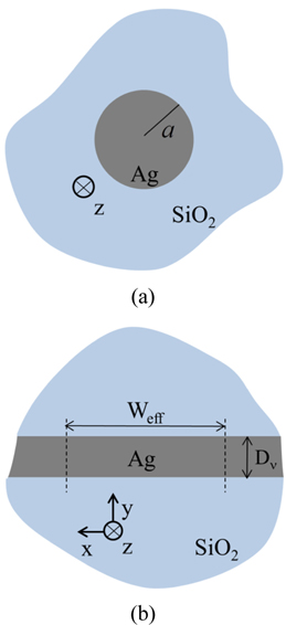
    An infinitely long and straight Ag NW (with radius a) was oriented along the z-axis and surrounded by silica as illustrated in Fig. 1(a). We found the modal dispersion relation of the Ag NW by building a relationship with the planar insulator-metal-insulator (IMI) geometry as shown in Fig. 1(b). It is worth noting that there has been previous work to investigate the surface plasmon propagation and confinement in IMI geometry [22]. Solving Maxwell’s equations using the boundary conditions for the IMI geometry, we obtained the dispersion relation (details are given in the Appendix.),

    where , k0 = ω/c is the free-space wavevector, εm , εd are the relative permittivity in the Ag and SiO2, respectively. The dielectric constant for Ag is taken from experimental data [21], the real-valued dielectric constant for SiO2 is fixed to (1.47)2. The effective thickness of the metal layer Dν is expressed by

    where ν is the mode order. The propagating mode in the Ag NW is influenced by the finite cross-sectional area of NW, however, the propagating mode in the IMI geometry is infinitely extended in the x-direction. Therefore we needed to define the effective width along to the x-axis to build an equivalent relationship with Ag NW, and we assumed that the cross-sectional area of the NW was equal to the effective metal area of the IMI geometry, described by

    for the fundamental mode. Here, Weff is defined as a perimeter of an effective mode area for fundamental mode, that is to say Weff = 2π(a+δ), where δ represents the effective field radius and defined as the distance required for the electric field intensity to decay by a factor of 1/e along the radial direction of the Ag NW, as shown in the inset image of Fig. 2. We assumed that the propagating mode had its total wavevector determined by the IMI dispersion relation,

    where β is the component of the wavevector along the propagating axis of the Ag NW [15, 17]. Combining Eqs. (1)-(4), we obtain the equivalent dispersion relation for the Ag NW, described by

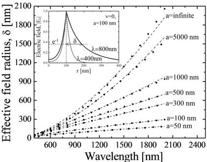
    To obtain the effective field radius δ , we used a direct a direct solution of the dispersion relation of the Ag NW obtained by solving Maxwell’s equation in cylindrical coordinates, as follows [23]:

    where Jν is a Bessel function of the first kind, is a derivative of Jν, K ν is a modified Bessel function of the second kind, is a derivative of K ν, , .

    The propagation constant β was calculated by solving Eq. (6). Using these results, we obtained the radial depen-dence of the z-components of the electric field and the δ as shown in inset image of Fig. 2. Figure 2 shows the effective field radius δ as a function of the radius a and the wavelength λ. The δ obtained from Eq. (6) is indicated by the black dots. The analytical expression indicated by the black dashed lines was obtained by a fitting of the δ obtained from Eq. (6) and is described by

    where A=0.01349, B=33.55, and τa=611.6. Here, f (a) = f(1-γ1e-a/a01 - γ2e-a/a02 where f=1.58587, γ1=0.4437, a01=1499.3, γ2=0.1271, and a02=66.2.

    III. RESULTS AND DISCUSSION

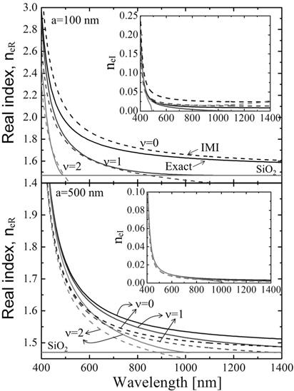
    The complex values of the effective refractive index ne = neR + ineI are yielded from Eq. (5) and (6). Figure 3 shows the effective refractive index of the first three azimuthal mode orders as a function of the wavelength. The top panel shows the real and imaginary parts of the effective refractive index for a radius of 100 nm, and the bottom panel shows the same for a radius of 500 nm. For a radius of 100 nm, the real part of the effective refractive index for the exact solution was in good agreement with that for our approximate value in the 400-1400 nm wave-length range. Small discrepancies were noticed between the exact and approximate solutions for the imaginary part of the effective refractive index (shown in the inset of the top panel of Fig. 3. For a radius of 500 nm, the real and imaginary parts of the effective refractive index for the exact solution were in good agreement with those for our approximate value in the 400-1400 nm wavelength range.

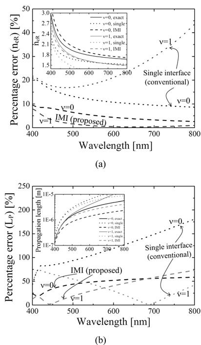
    We now examine in detail the percentage error of the real part of the effective refractive index and the propagation length in the 400-800 nm wavelength range as shown in Fig. 4. For the real part of the effective refractive index, the percentage error (neR) is defined by 100×(| neR,exact - neR, approx. | / neR,exact), and the approximated model proposed is low-value for the whole wavelength range compared with the previous planar metal-insulator geometry as shown in Fig. 4(a) [17]. The average percentage error for the fundamental mode was reduced to 5% compared with the previous result of 11.9%, and that for the 1st order mode was reduced to 1.5% compared with the previous result of 24.8%.

    Figure 4(b) shows the percentage error (LP) of the propagation length. The propagation length is given by LP = 1 / (2nelk0) and the percentage error (LP) is defined by 100×(| LP,exact - LP, approx. | / LP,exact). The average percentage error for the fundamental mode was reduced to 48% compared with the previous result of 121.5%, and that for the 1st order mode was slightly increased 39.4% compared with the previous result of 36.2%.

    IV. CONCLUSION

    In summary, we proposed a simple model to elucidate the dispersion behavior of spiraling modes on Ag NW by building a relationship with the planar IMI geometry. The previous model with planar metal-insulator geometry has large discrepancies compared with the exact solution when the radius of NW is compatible with the skin depth, due to interactions with the electric field around the NW. Our equivalent model solved this problem by introducing plasmon modes that exist on thin metal films sandwiched between two regions of identical dielectrics, and the percentage error was remarkably reduced. This approach provides important insights into the behavior of NW wave-guides. In addition, it has much broader applicability than the previous model and it can be extended to provide insights into more complicated NW-based waveguides.

참고문헌
  • 1. Raether H. 1998 Surface Plasmons on Smooth and Rough Surfaces and on Gratings google
  • 2. Dionne J.A., Sweatlock L.A., Atwater H.A., Polman A. 2006 “Plasmon slot waveguides: Towards chip-scale propagation with subwavelength-scale localization,” [Phys. Rev. B] Vol.73 P.035407 google cross ref
  • 3. Chen J., Smolyakov G.A., Brueck S.R.J., Malloy K.J. 2008 “Surface plasmon modes of finite, planar, metal-insulator-metal plasmonic waveguides,” [Opt. Express] Vol.16 P.14902-14909 google cross ref
  • 4. Bozhevolnyi S.I., Volkov V.S., Devaux E., Laluet J.-Y., Ebbesen T.W. 2006 “Channel plasmon subwavelength waveguide components including interferometers and ring resonators,” [Nature] Vol.440 P.508-511 google cross ref
  • 5. Liu L., Han Z., He S. 2005 “Novel surface plasmon waveguide for high integration,” [Opt. Express] Vol.13 P.6645-6650 google cross ref
  • 6. Berini P., Charbonneau R., Lahoud N., Mattiussi G. 2005 “Characterization of long-range surface-plasmon-polariton waveguides,” [J. Appl. Phys.] Vol.98 P.043109 google cross ref
  • 7. Berini P. 2001 “Plasmon-polariton waves guided by thin lossy metal films of finite width: Bound modes of asymmetric structures,” [Phys. Rev. B] Vol.63 P.125417 google cross ref
  • 8. Berini P. 2000 “Plasmon-polariton waves guided by thin lossy metal films of finite width: Bound modes of symmetric structures,” [Phys. Rev. B] Vol.61 P.10484-10503 google cross ref
  • 9. Holmgaard T., Chen Z., Bozhevolnyi S.I., Markey L., Dereux A. 2009 “Dielectric-loaded plasmonic waveguide-ring resonators,” [Opt. Express] Vol.17 P.2968-2975 google cross ref
  • 10. Dai D., He S. 2009 “A silicon-based hybrid plasmonic waveguide with a metal cap for a nano-scale light confinement,” [Opt. Express] Vol.17 P.16646-16653 google cross ref
  • 11. Dai D., He S. 2010 “Low-loss hybrid plasmonic waveguide with double low-index nano-slots,” [Opt. Express] Vol.18 P.17958-17966 google cross ref
  • 12. Su Y., Zheng Z., Bian Y., Liu L., Zhao X., Liu J., Zhou T., Guo S., Niu W., Liu Y., Zhu J. 2012 “Metal-coated hollow nanowires for low-loss transportation of plasmonic modes with nanoscale mode confinement,” [J. Optics-UK] Vol.14 P.095501 google cross ref
  • 13. Krasavin A.V., Zayats A.V. 2010 “Silicon-based plasmonic waveguides,” [Opt. Express] Vol.18 P.11791-11799 google cross ref
  • 14. Karalis A., Lidorikis E., Ibanescu M., Joannopoulos J.D., Soljacic M. 2005 “Surface-plasmon-assisted guiding of broadband slow and subwavelength light in air,” [Phys. Rev. Lett.] Vol.95 P.063901 google cross ref
  • 15. Catrysse P.B., Fan S. 2009 “Understanding the dispersion of coaxial plasmonic structures through a connection with the planar metal-insulator-metal geometry,” [Appl. Phys. Lett.] Vol.94 P.231111 google cross ref
  • 16. Wang W., Yang Q., Fan F., Xu H., Wang Z.L. 2011 “Light propagation in curved silver nanowire plasmonic waveguides,” [Nano Lett.] Vol.11 P.1603-1608 google cross ref
  • 17. Schmidt M.A., Russell P. St. J. 2008 “Long-range spiralling surface plasmon modes on metallic nanowires,” [Opt. Express] Vol.16 P.13617-13623 google cross ref
  • 18. Wei H., Xu H. 2012 “Nanowire-based plasmonic waveguides and devices for integrated nanophotonic circuits,” [Nanophotonics] Vol.1 P.155-169 google
  • 19. Li Q., Qiu M. 2013 “Plasmonic wave propagation in silver nanowires: guiding modes or not?” [Opt. Express] Vol.21 P.8587-8595 google cross ref
  • 20. Wang Y., Ma Y., Guo X., Tong L. 2012 “Single-mode plasmonic waveguiding properties of metal nanowires with dielectric substrates,” [Opt. Express] Vol.20 P.19006-19015 google cross ref
  • 21. Palik E.D. 1985 Handbook of Optical Constants of Solids google
  • 22. Dionne J.A., Sweatlock L.A., Atwater H.A., Polman A. 2005 “Planar metal plasmon waveguides: frequency-dependent dispersion, propagation, localization, and loss beyond the free electron model,” [Phys. Rev. B] Vol.72 P.075405 google cross ref
  • 23. Okamoto K. 2006 Fundamentals of Optical Waveguides google
OAK XML 통계
이미지 / 테이블
  • [ FIG. 1. ]  (a) An infinitely long and straight Ag NW (radius a) is oriented along the z-axis and surrounded by silica. (b) The proposed equivalent model with planar insulator-metal-insulator (IMI) geometry.
    (a) An infinitely long and straight Ag NW (radius a) is oriented along the z-axis and surrounded by silica. (b) The proposed equivalent model with planar insulator-metal-insulator (IMI) geometry.
  • [ FIG. 2. ]  The effective field radius δ as a function of the radius and the wavelength. The black dots are obtained from an exact solution (Eq. (6)) and the black dashed lines are obtained from our analytical solution (Eq. (7)). The inset shows the radial dependence of the z-components of the electric field for ν =0 and a =100 nm at wavelengths of 400 nm and 800 nm.
    The effective field radius δ as a function of the radius and the wavelength. The black dots are obtained from an exact solution (Eq. (6)) and the black dashed lines are obtained from our analytical solution (Eq. (7)). The inset shows the radial dependence of the z-components of the electric field for ν =0 and a =100 nm at wavelengths of 400 nm and 800 nm.
  • [ FIG. 3. ]  The effective refractive index of the first three azimuthal mode orders as a function of the wavelength. The real and imaginary parts of the effective refractive index (top panel) for a radius of 100 nm and (bottom panel) for a radius of 500 nm. The grey solid line corresponds to the bulk material refractive index of SiO2.
    The effective refractive index of the first three azimuthal mode orders as a function of the wavelength. The real and imaginary parts of the effective refractive index (top panel) for a radius of 100 nm and (bottom panel) for a radius of 500 nm. The grey solid line corresponds to the bulk material refractive index of SiO2.
  • [ FIG. 4. ]  (a) The percentage error ( neR ) for the real part of the effective refractive index in the 400-800 nm wavelength range. The dashed lines and the dotted lines correspond to the proposed IMI geometry and the previous metal-insulator geometry, respectively. Inset shows the effective refractive index as a function of the wavelength from the exact solution (solid lines), previous metal-insulator geometry (dotted lines), and proposed IMI geometry (dashed lines). (b) The percentage error (LP) of the propagation length in the 400-800 nm wavelength range. Inset shows the propagation length as a function of the wavelength from the exact solution (solid lines), previous metal-insulator geometry (dotted lines), and proposed IMI geometry (dashed lines).
    (a) The percentage error ( neR ) for the real part of the effective refractive index in the 400-800 nm wavelength range. The dashed lines and the dotted lines correspond to the proposed IMI geometry and the previous metal-insulator geometry, respectively. Inset shows the effective refractive index as a function of the wavelength from the exact solution (solid lines), previous metal-insulator geometry (dotted lines), and proposed IMI geometry (dashed lines). (b) The percentage error (LP) of the propagation length in the 400-800 nm wavelength range. Inset shows the propagation length as a function of the wavelength from the exact solution (solid lines), previous metal-insulator geometry (dotted lines), and proposed IMI geometry (dashed lines).
(우)06579 서울시 서초구 반포대로 201(반포동)
Tel. 02-537-6389 | Fax. 02-590-0571 | 문의 : oak2014@korea.kr
Copyright(c) National Library of Korea. All rights reserved.