A split-step time-domain model for the analysis of pulse delay characteristics through ring resonator all-pass filters (APF’s) is developed and its accuracy is checked. The dependence of the delay time and pulse distortion on the coupling ratios is investigated using the model. It is observed that the bandwidth of the APF's needs to be wide enough to minimize the pulse distortion.
As the demand for high-speed communication both in wired and in wireless systems increases, the optical fiber communication systems have been developed in such a way that the information transmission capacity through an optical fiber exceeds terabits per second. As the data speed increases, the packet switching network is expected to advance from electronic packet switching to all-optical packet switching networks in which electrical-to-optical and optical-to-electrical conversions are not involved. In the all-optical packet switching networks, optical packets carried in a specific wavelength channel can be routed to a destination transparently, thus the network can be expanded flexibly when necessary [1-2]. Furthermore, optical packet switching system might be adopted in optical interconnection technology for high-speed signal transmission as the VLSI (Very Large System Integration) circuits become extremely integrated [3].
In the all-optical packet switching or optical interconnection system, optical switches and variable optical delay modules are required. There have been a variety of approaches to realize optical delay modules [4-16]. A CROW (Coupled resonator optical waveguide) [5-8] has drawn interest for all-optical packet communication or optical signal processing modules because it can reduce the propagation speed variably. The CROW can be implemented in the form of Fabry-Perot, photonic crystal, or ring resonators, etc. Among them, the CROW based on ring resonators have shown noticeable advances in practical realization in terms of design and fabrication feasibility [7].
Even though several approaches in analytical and numerical analysis of the CROW’s provides lots of information regarding the delay performance of the devices [17-19], the quality of delayed pulse shapes can be directly investigated through a time-domain analysis.
In this paper, an efficient split-step time-domain approach for the numerical analysis of the ring resonator devices such as CROW devices is presented [20-21]. The numerical algorithm is illustrated through the analysis of single-, double-, triple-, and quadruple-ring resonator all-pass filters, which can be extended to general CROW-type devices with arbitrary number of rings. In section II, the split-step time-domain algorithm is elaborated. In section III, the accuracy of the numerical approach is checked, and the delay characteristics of single-, double-, triple- and quadruplering all-pass filter (CROW device) are investigated and some design guidelines are presented. Finally, conclusions are given.
II. FORMULATION OF TIME-DOMAIN MODEL FOR RING RESONATOR ALL PASS FILTER
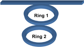
A double-ring resonator all-pass filter (APF) shown in Fig. 1 is considered to explain the time-domain model employed in this paper. For the time-domain analysis of the ring resonator, a split-step time-domain model (SSTDM) is developed [20-21]. In this model, the numerical solution of the time-dependent coupled-wave equation is found through a split-step operator approach. The SS-TDM consists of the numerical solution of the time-dependent coupled-wave equations for the forward and reverse waves.
The optical field within waveguides can be written as
where
where
In this paper, passive waveguides are considered and, thus
where
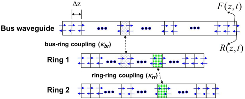
For the analysis, three sets of time-dependent coupledwave equations are used because three waveguides exist in the structure. Fig. 2 shows the conceptual configuration considered for the simulation. The couplings between waveguides occur at particular sections in three waveguides. The ring (circular) waveguides are assumed to be bus waveguides which require the following periodic boundary conditions :
The boundary condition for the bus waveguide is given as
The time-dependent coupled-wave equations can be numerically solved by dividing the waveguides into a number of small subsections having equal length (Δz) as shown in Fig. 2. In the simulation, the calculation in each section (Δz) consists of two operations which are performed for Δt (=Δz/cg). First, the forward/reverse waves in three waveguides (a bus and two ring waveguides) are updated to incorporate the attenuation and phase accumulation through a section (Δz) in a time step (Δt). Then, the coupling effects between waveguides are taken into consideration. The split-step algorithm is computerized through the following procedure:
(1) The waveguides are divided into a number of small subsections having equal length (Δz ).(2) The photon density in each section of three waveguides is updated using the following timestepping equation:
(3) The coupling effects between waveguides are taken into consideration. For example, the coupling effect between the bus and ring 1 can be incorporated using
Here, the subscripts 1 and 2 represent the field amplitudes in bus and ring 1 waveguides, respectively. In the above equations, zb indicates the position of coupling with ring 1 in the bus waveguide. Similarly, zrl indicates the position of coupling with bus in ring 1. The distributed coupling of the directional coupler is assumed to occur at zb and zrl in a lumped way. The parameter K12 is the total coupling ratio through the directional coupler between two waveguides 1 and 2, and T is the total straightthrough ratio given by {}. The coupling between two rings is also incorporated similarly.
(4) The appropriate boundary conditions (4) in the bus and ring waveguides are applied at every time step.
III. NUMERICAL RESULTS AND DISCUSSIONS
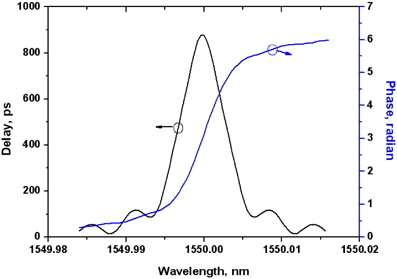
The numerical model described in Section II can be checked by comparing the phase and delay responses as a function of wavelength calculated from the numerical model with the analytical and numerical spectral analysis [17-19] for a single-ring resonator APF. The waveguide is assumed to be lossless throughout the discussions in this section. The perimeter of the ring is set to be 2000m and the group refractive index of the material 1.5. For this ring, the FSR (Free Spectral Range) is calculated to be 100GHz and the round-the-ring trip delay along the ring is 10ps. The coupling ratio between the bus and the ring is set to be 0.5 in this case. For the calculation, the continuous wave with varying wavelengths are launched into the single-ring APF and the output phase is measured for each wavelength. Then the delay time is calculated using a formula where Ø is a phase through the APF and
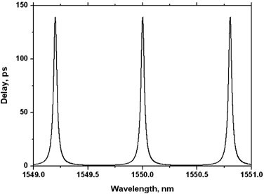
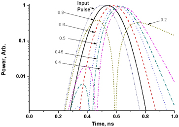
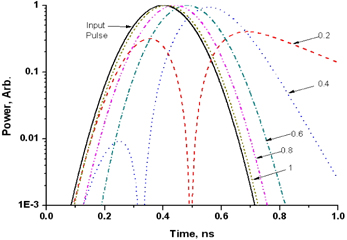
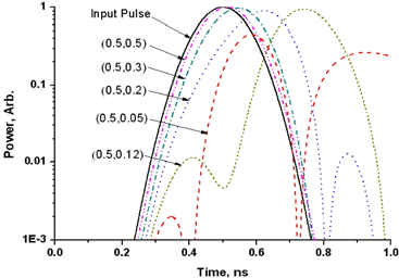
The delayed waveform of the 167ps-wide (FWHM: Full Width at Half Maximum) input optical pulse through the single-ring resonator APF is shown in Fig. 5. The input pulse has no chirp. The delay time increases as the coupling ratio decreases. When the coupling ratio is one, the delay time is about 10ps which is the same as the round-the-ring trip delay along the single ring resonator. When the coupling ratio is 0.5, the delay time is about 110ps, which is smaller than the peak delay time of 138ps shown in Fig. 3. The spectral width of the unchirped 167ps (FWHM) optical pulse is about 2.63GHz (0.021 nm) [22]. Considering the spectral width of the input optical pulse, the delay time of 110ps seems to be appropriate for the delay time spectrum as shown in Fig. 3. When the coupling ratio is 0.4, the delay time is about 145ps while the spurious pulse amplitude is about -17dB of the main pulse. In order to suppress the spurious pulse amplitude below -30dB, the coupling ratio should be larger than 0.5. Fig. 5 also shows that the spurious pulse amplitude is almost the same as the main pulse when the coupling ratio is 0.2. This can be understood from the phase and delay time calculation as a function of wavelength as shown in Fig. 6. The FWHM bandwidth of the delay response is only 0.006 nm (0.75 GHz) which is too narrow for the 167ps pulse to pass through without distortion.
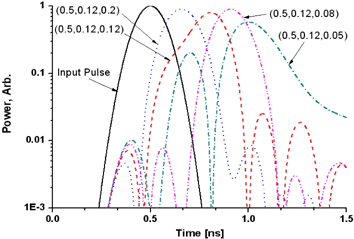
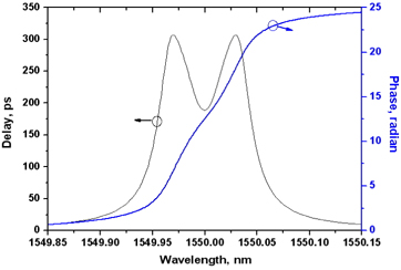
The delayed waveform for the input optical pulse of 250ps (FWHM) is shown in Fig. 7. The delay characteristics are similar to the case of 200ps input pulse, except that the spurious pulse amplitudes are smaller. In Fig. 8, the delayed waveform through a double ring resonator APF is shown for various values of the ring-ring coupling ratios with the bus-ring coupling ratio fixed to be 0.5. When the ring-ring coupling ratio is 0.1, the maximum delay of 280ps is observed with the spurious pulse amplitude to be -20 dB of the main pulse amplitude. In Fig. 9, the delayed waveform through a triple ring resonator APF is shown for various values of the second ring-ring coupling ratios with the bus-ring coupling ratio and the first ring-ring coupling ratio fixed to be 0.5 and 0.12, respectively. When the second ring-ring coupling ratio is 0.08, the maximum delay of 408ps is observed with the spurious pulse amplitude smaller than -20dB of the main pulse amplitude.
The delay characteristics for the chirped pulse also need to be investigated. The electric field of linearly chirped optical pulse is expressed as follows [22]:
In the above, α is the linewidth enhancement factor and
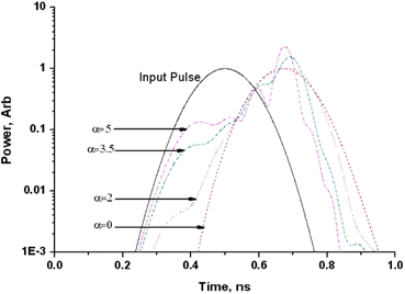
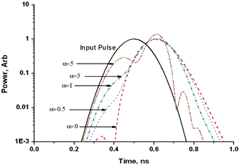
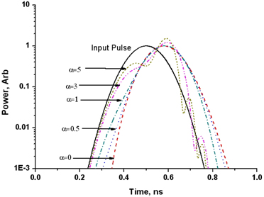
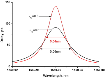
The pulse width corresponding to 1% of the peak is about 500ps for the 167ps (FWHM) optical pulse. For this time span, the frequency variation is 8GHz (0.064 nm) in case of α = 1. This fact illustrates that the bandwidth of the APF with the coupling ratio of 0.5 is not wide enough to delay the leading and trailing edges of the pulse below 1% of the pulse peak. When the coupling ratio is increased from 0.5 to 0.6, the bandwidth is increased from 0.04 nm to 0.06 nm. As a result of the bandwidth increment, the pulse is delayed without severe distortion for the APF with the coupling ratio of 0.6. In both cases, the bandwidth delay product (Δν · Δτ
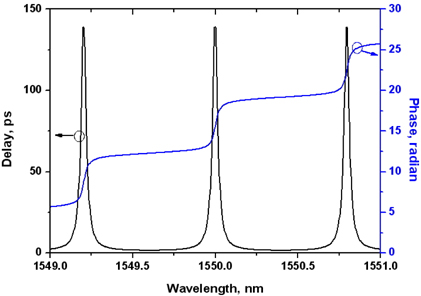
An APF composed of four coupled rings are also considered to investigate the effect of the bandwidth on the distortion of the input pulse. The coupling ratios are apodized to increase the bandwidth. The bus-ring coupling ratio is 0.8, the ring-ring coupling ratios are 0.34, 0.19, and 0.17. The delay characteristics are shown in Fig. 13. It is observed that the pulse delay of 175ps is achieved without severe distortion even for α = 2. This result comes from the widened bandwidth as shown in Fig. 14. The bandwidth delay product (Δν · Δτ
A split-step time-domain modeling approach is developed to analyze the ring resonator delay devices. In this approach, the optical field evolution in terms of phase and loss is incorporated in the small section and then the directional coupling effect is taken into consideration at each time step. For the bus and the rings, appropriate boundary conditions are applied at each time step. The accuracy of the split-step time-domain analysis is checked by comparing with the spectral analysis using an analytical solution. The time-domain model is applied to analyze the optical pulse transfer characteristics through single-, double-, and triple-ring APF’s. In the single-ring APF, the pulse delay increases as the coupling ratio decreases. On the other hand, the pulse shape distortion becomes worse as the coupling ratio decreases, which comes from the reduction of bandwidth for lower coupling ratio. As the number of rings are increased with optimum coupling ratios, the delay time scales with the number. For the single-ring, double-ring, and triple-ring APF with 100GHz free spectral range, the delay is 140ps, 280ps, and 408ps, respectively. The pulse transfer characteristics through the single-ring and apodized quadruple-ring APF for the chirped pulse are also studied. It is observed that the bandwidth of the APF should be wide enough to minimize the pulse shape distortion. With these examples it is shown that the split-step time-domain model is useful to efficiently analyze the pulse distortion through the ring resonator delay devices in detail and can be incorporated into an advanced optical communication modeling software in the future.