This paper presents a characteristic evaluation of commercial gallium nitride (GaN) transistors having two different gate-lengths of 0.4-μm and 0.25-μm in the design of a class-S power amplifier (PA). Class-S PA is operated by a random pulse-width input signal from band-pass delta-sigma modulation and has to deal with harmonics that consider quantization noise. Although a transistor having a short gate-length has an advantage of efficient operation at higher frequency for harmonics of the pulse signal, several problems can arise, such as the cost and export license of a 0.25-μm transistor. The possibility of using a 0.4-μm transistor on a class-S PA at 955 MHz is evaluated by comparing the frequency characteristics of GaN transistors having two different gate-lengths and extracting the intrinsic parameters as a shape of the simplified switch-based model. In addition, the effectiveness of the switch model is evaluated by currentmode class-D (CMCD) simulation. Finally, device characteristics are compared in terms of current-mode class-S PA. The analyses of the CMCD PA reveal that although the efficiency of 0.4-μm transistor decreases more as the operating frequency increases from 955 MHz to 3,500 MHz due to the efficiency limitation at the higher frequency region, it shows similar power and efficiency of 41.6 dBm and 49%, respectively, at 955 MHz when compared to the 0.25-μm transistor.
Enhancement of the efficiency of the power amplifier (PA) at a wide dynamic range is important for modern communication signals. Various groups have studied several efficiency enhancement techniques, such as Doherty [1-4], envelope tracking [5,6], envelope elimination and restoration [7], and linear amplification with nonlinear components [8]. The class-S amplifier and the concept of digital amplifier based on the delta-sigma modulator (DSM) and switch-mode PA (SMPA) with push-pull structure, is now being intensively investigated because the class-S system has potential to provide high linearity and efficiency [9,10].
However, the overall characteristics of a PA, such as the output power, efficiency, and operating frequency, are basically decided by the transistor. Therefore, the selection of the transistor is important in the design of a PA. The SMPA, in particular, requires a transistor capable of high power and speed when working in the range of radio frequencies (RF). The purely digital operation of the class-S PA also requires a fast switching transistor, and several studies on class-S PA using gallium nitride (GaN) transistor are in progress.
The increased demand for high power and frequency has led to intensive study and wide use of GaN in many fields. GaN has excellent characteristics such as a wide band gap, high breakdown voltage, high thermal conductivity, and high electron saturation velocity [11-15]. Above all, the high power capability of GaN enables low intrinsic capacitance and fast switching operation [16,17], and many studies on transistor structure are now actively investigating ways to achieve efficient operation at higher frequency by reducing gate-length of transistor. A 0.4-μm transistor is now in wide use and a 0.25-μm transistor is also available on the market. However, although a transistor with a short gate-length will clearly show better performance at higher frequency, some problems still limit the use of the 0.25-μm transistor, such as its cost and export license.
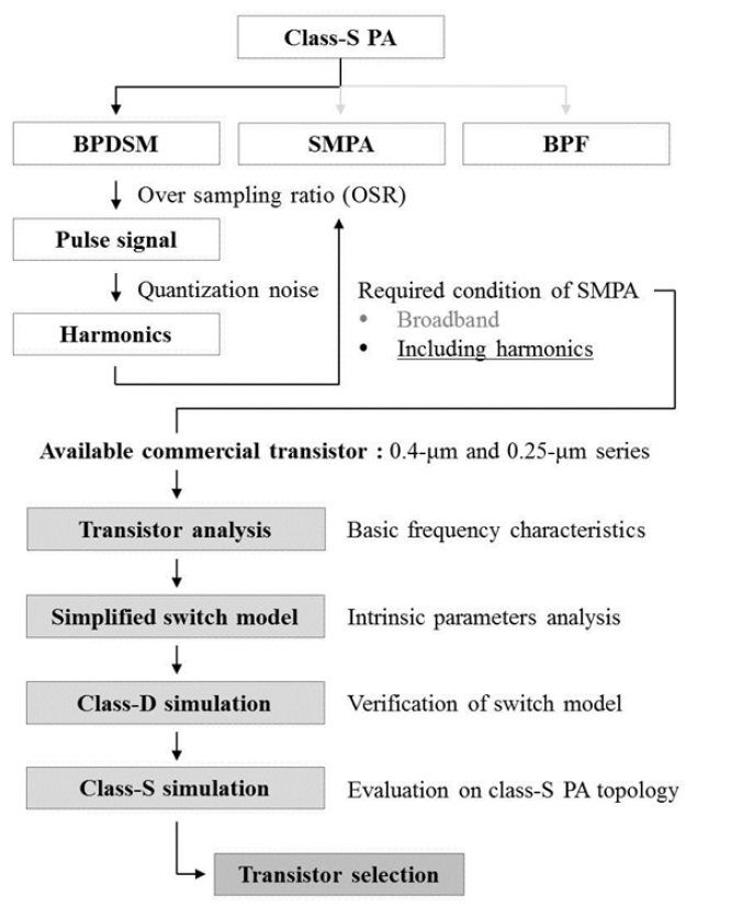
In this paper, the possibility of using a transistor having a 0.4-μm gate-length on a class-S PA at 955 MHz in comparison to a 0.25-μm transistor is evaluated by examining the small-signal characteristics, such as maximum available gain as well as current gain, using a commercial GaN transistor having two different gate-lengths and similar output power. The intrinsic parameters of the GaN transistor are extracted as the simplified switch-based model and the basic RF characteristics of the simplified switch model and behavior transistor model are described by load-pull simulation. The device characteristics are analyzed in terms of current-mode class-D (CMCD) and current-mode class-S (CMCS) PA structures. This paper is organized as shown in Fig. 1.
III. SIMPLIFIED SWITCH-BASED MODEL OF A GAN TRANSISTOR
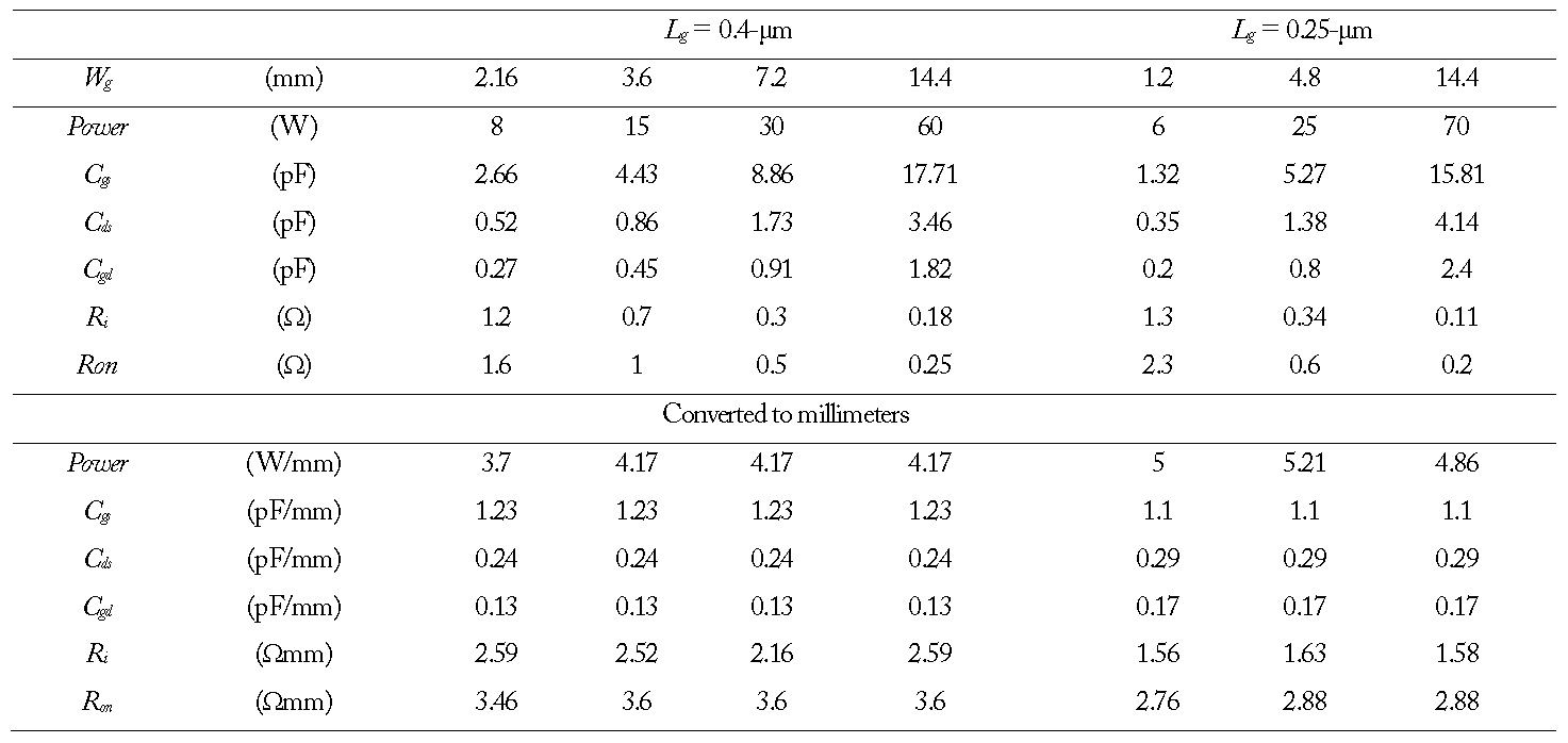
Generally, the gate-width and gate-length of a transistor are related to an output power and a maximum operating frequency, respectively. As high frequency operation of transistors is required in many fields, research has mainly focused on reducing the transistor gate-length. Considering this trend, the simulation models by CREE Inc., which utilize GaN transistors with two different gate lengths of 0.4-μm and 0.25-μm, are used to evaluate the characteristics of the transistor in terms of CMCD and CMCS PA. The effect of transistor size is examined by using transistors with various gate dimensions in each case. Note that the gate-widths of these transistors are unequal and specific width is used for the two gate-lengths, because these transistors are commercial transistors, used to select an adequate one for CMCS PA. This section introduces the DC and RF characteristics of transistors to confirm the frequency responses according to the gate-length for harmonics of a pulse-shaped input signal.
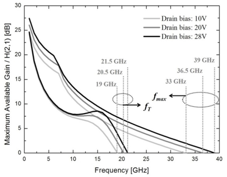
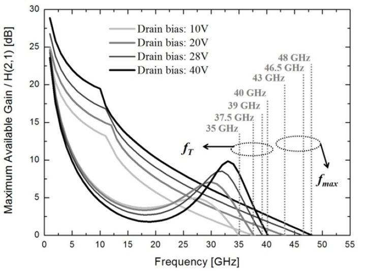
1. DC Characteristics: ?T and ?max
The operation of the transistor from the perspective of frequency variation can be simply shown as a unity current gain frequency (
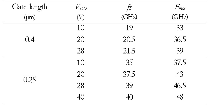
?T and ?max characteristics of GaN transistors with a gate-length of 0.4-μm and 0.25-μm according to the drain bias voltages
2. RF Characteristics: Load-Pull Simulation
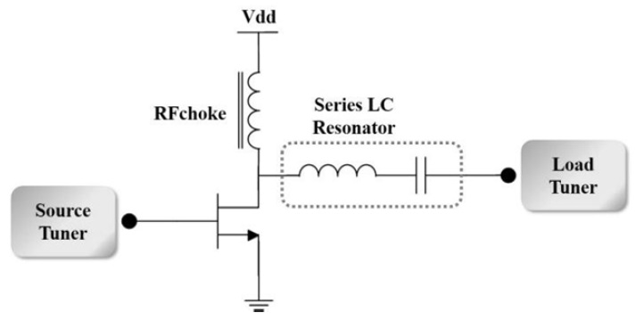
In general, large signal characteristics of transistors can be extracted by load-pull simulation. For the SMPA design, the performance of a class-D PA can also be obtained by load-pull simulation with a proper harmonic termination, as shown in Fig. 4. In this conventional class-D topology, the series LC resonator resonates on an operating fundamental frequency, and thereby terminates harmonics as an open condition. Note that in order to achieve proper class-D operation and have open-state harmonics, the effects of
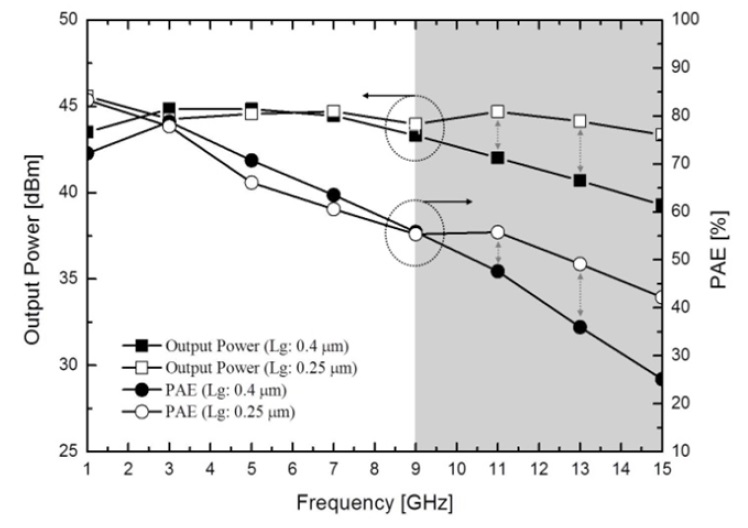
From the simulation in the frequency range between 1 GHz to 15 GHz, the output power and power-added efficiency (PAE) characteristics of the transistor are simulated and described in Fig. 5. GaN transistors are used that have gate-lengths of 0.4-μm and 0.25-μm and maximum power outputs of 30 W and 25 W, respectively. Although the results are similar in the frequency ranges under 9 GHz, the performance differences of the two transistors become obvious as frequency increases. Thus, the device with a short gate-length is clearly advantageous for high frequency applications.
III. SIMPLIFIED SWITCH-BASED MODEL OF A GAN TRANSISTOR
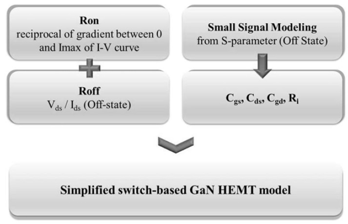
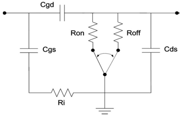
The conventional linear amplifiers such as class-A, AB, B, and C are generally designed by using the behavioral model from the manufacturer or by measuring source and load impedances. However, this large signal model is complicated and needed a lot of time to simulate, whereas the SMPA operates in only two states, the on- and off-states. Therefore, the simplified switchbased model is sufficient to predict the switching operation of CMCD PA and has been studied by several groups [8-20]. The simplified switch-based model in the desired bias condition can be extracted by small-signal modeling of FET, which was pro posed in 1988 by Dambrine et al. [21]. Fig. 6 briefly shows the modeling procedure of the simplified switch-based model. The on- and off-resistances are calculated by the inverse number of gradient between voltage and current value in the I-V curve of transistor. The intrinsic capacitances,

Summary of the intrinsic parameters of gallium nitride (GaN) transistors with a gate-length of 0.4-μm and 0.25-μm according to the different gate-widths
The simplified switch-based model of GaN transistor is composed of the calculated values, as shown in Fig. 7. According to the input voltage level, the switch in this model is set with
IV. CHARACTERISTICS OF CMCD AND CMCS PAS
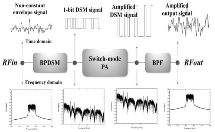
The class-S power amplifier consists of a band-pass delta sigma modulator, SMPA, band-pass filter, and balun. Fig. 8 shows the spectra and waveforms of the conventional class-S system according to the each stage. In the constituent of class-S PA, SMPA is the most important part and has some required conditions, such as broad-band matching, push-pull operation, and high-speed switching ability. This SMPA must be enabled to operate at a higher frequency range for the over sampling ratio (OSR) needed to generate the pulse waveform.
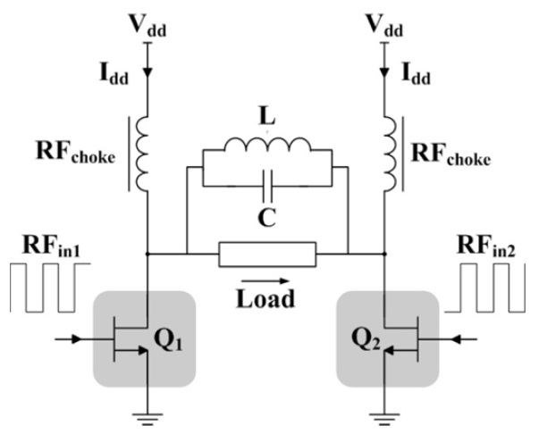
Two different structures, generally called current-mode and voltage-mode and derived from the conventional class-D amplifier, are suitable for the SMPA. For a high power operation, when compared to the voltage-mode, the current-mode operation has several advantages of including the elimination of drainsource capacitance, simple driver circuitry, and the convenience of using the transistor without considering a stacked structure. Therefore, in this section, transistors with gate-lengths of 0.4-μm and 0.25-μm and similar output power characteristics, and with gatewidths of 7.2 mm and 4.8 mm, respectively, are evaluated by simulation on the structure of a CMCD PA.
1. CMCD PA Simulation at 955 MHz
A simple schematic for the CMCD PA for simulation is shown in Fig. 9. The simplified switch-based models of GaN transistors with two different gate-lengths of 0.4-μm and 0.25-μm are used at the position of
The pulse input signals corresponding to 955 MHz are complementarily injected to each transistor and enabled PA to the push-pull operation. The input signals are amplified efficiently through the switching transistors, and the final RF signal is extracted from the amplified output pulse signal by using the parallel LC resonator. The LC resonator sets a resonance frequency to an operating frequency, and thereby harmonics are filtered and adequately terminated. From the simulation at the input pulse signal of 955 MHz, the result of the simplified switch-based model shows a good agreement with that of the behavioral model from the perspective of output power and drain efficiency. Although a short gate-length transistor is advantageous at high frequency operation as shown in the previous section, the 0.4-μm GaN transistor in the CMCD PA structure shows a better efficiency at 955 MHz owing to the low on-resistance. Table 3 describes the characteristics of the CMCD PA structure using the simplified switch-based model and behavioral model at 955 MHz. Note that when the pulse signal is applied at the input of the transistor, the power is lost in charging and discharging the input capacitor. Although this factor has to be considered in the design of the CMCD PA, it is minimized in this simulation by assuming low input resistance to prevent distortion of pulse signal. Therefore, two limitations at the input of the transistor, namely broadband and low resistance, have to be considered in the fabrication of the CMCD PA.
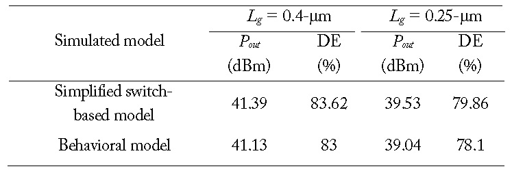
Characteristics of CMCD PA using the simplified switchbased model and behavioral model of GaN transistors with a gate-length of 0.4-μm and 0.25-μm at 955 MHz
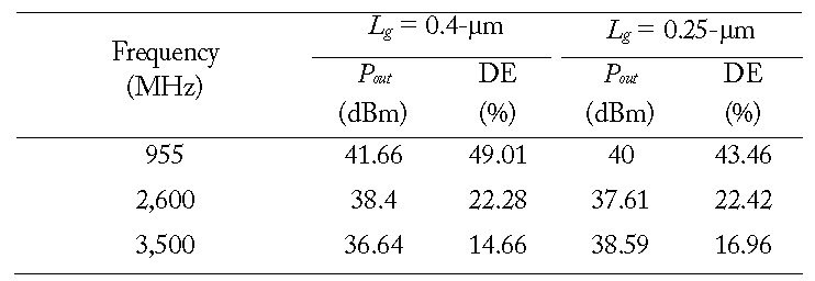
2. CMCS PA Simulation at 955, 2,600, and 3,500 MHz
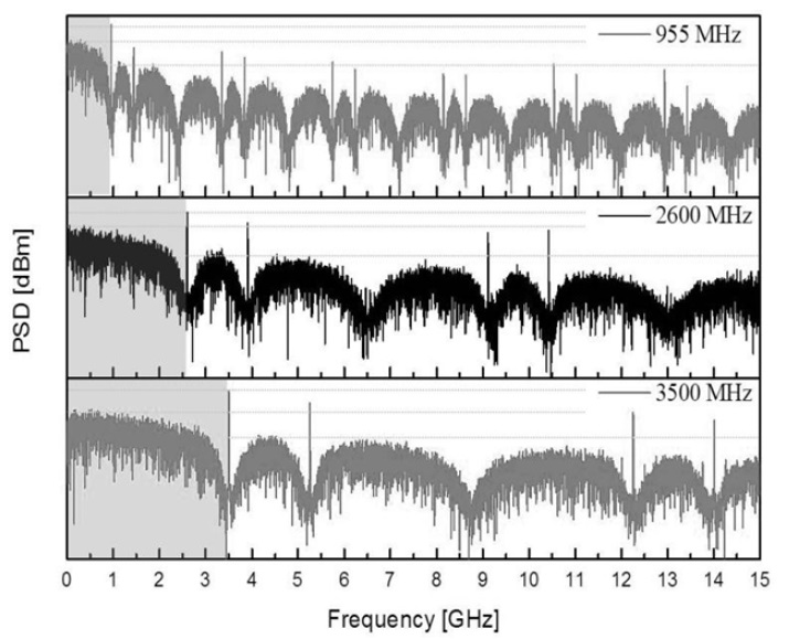
The non-constant RF input signal is converted into a 1-bit random pulse-width modulated signal by the BPDSM, which enables the SMPA to perform the push-pull operation. The CMCS PA amplifies the differential BPDSM input signal, and due to the pulse shaped BPDSM input signal, the PA is required to have broadband characteristics up to several times the operating frequency, which is called OSR. The frequency component of the pulse is composed of fundamental frequency and harmonics, which result in quantization noise components of the BPDSM signals. The quantization noise levels are important to sustain BPDSM signal, and the shape of pulse directly influences the output power and efficiency of the class-S PA.
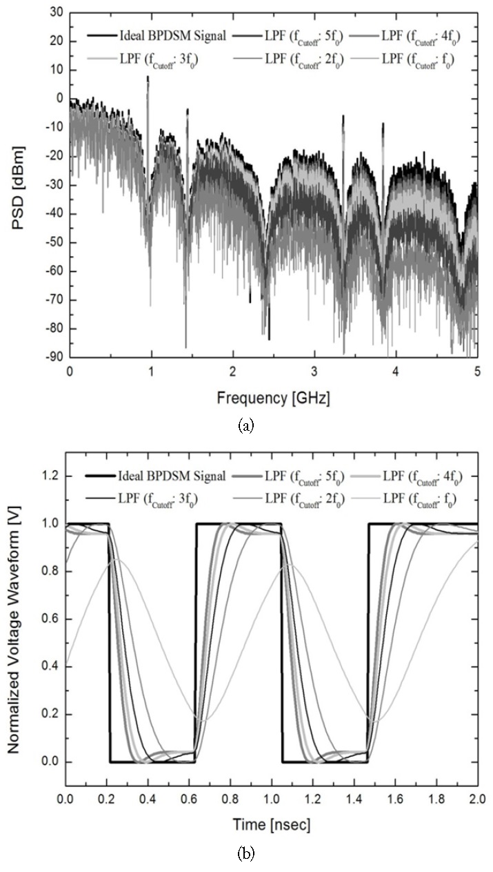
Fig. 10 shows the variations of spectra and waveforms of the BPDSM signal according to the upper cutoff frequency by assuming the bandwidth of the PA as a low-pass filter. That is, this graph illustrates the impact of high frequency harmonic components on the waveforms. When harmonic components are included as frequently as possible, the BPDSM signal can be similar to the ideal pulse signal. Therefore, at a minimum, the transistor for a CMCS PA has to have a gain until a frequency is reached that is three or four times the operating frequency.

Simulated characteristics of CMCS PA applying a BPDSM input signal using GaN transistors with a gate-length of 0.4-μm and 0.25-μm at three operating frequencies
A simulation of the conventional CMCS PA, applying a BPDSM input signal of 8.5 dB PAPR 3G LTE 10 MHz at three operating frequencies of 955, 2,600, and 3,500 MHz reveals that the characteristics of the PA using 0.4-μm and 0.25-μm GaN transistors can be expected considering the effect of the upper frequency limit of the transistor. Fig. 11 describes the BPDSM input signals with center frequency of 955, 2,600, and 3,500 MHz, and Table 4 is a summary of the simulated characteristics of the CMCS PA at three operating frequencies in terms of an average output power and efficiency. The 955 MHz is the desired frequency in this work, and both transistors having two different gate-lengths are available in the CMCS PA considering OSR and compared with each other. The other operating frequencies, 2,600 and 3,500 MHz, are also selected among the LTE frequencies to evaluate the characteristics of transistor according to the higher harmonics. As shown in Fig. 5, the 0.4-μm transistor does not operate as efficiently as the 0.25-μm transistor at higher frequency region and this trend is well reflected in Table 4. However, although the efficiency of the 0.4-μm transistor decreases to a greater extent as the operating frequency increases from 955 to 3,500 MHz due to the efficiency limitation at the higher frequency region, it shows better efficiency (as much as 5.5%) at 955 MHz compared to 0.25-μm transistor. Therefore, an adequate transistor has to be selected depending on desired operating frequency and its harmonics, and the 0.4-μm GaN transistor is more advantageous in the design of CMCS PA compared to the 0.25-μm transistor at 955 MHz. Note that these results are caused by the different gate-width of each commercial transistor with two gate-lengths for the desired output power. In fact, if the gate-width is identical, the transistor having a short gate-length will show better efficiency even at 955 MHz.
Based on the above analysis, we previously proposed two types of current-mode PAs, which are push-pull inverse class-F PA [22] and hybrid current-mode class-D PA [23]. In those papers, PAs attained a high efficiency (over 77%) in the frequency range of 3.3 GHz. In addition, a hybrid CMCS PA was also proposed using the chip-on-board technique for the 955 MHz LTE signal and showed an efficiency of 38.5% at the average power [24].
This paper describes a process for the selection of an adequate transistor among the commercial GaN transistors having two different gate-lengths for class-S PA design. First, the basic characteristics of the GaN transistor with two gate-lengths of 0.4-μm and 0.25-μm are analyzed by extracting