Due to their unique geometry and physical properties, carbon nanotubes (CNTs) are currently being investigated as next-generation field emitter materials for cold cathodes. Numerous papers can be found on field emission applications such as field emission displays, lamps, X-ray sources, high-resolution electron-beam instruments, and microwave amplifiers [1-5]. Up to now, various techniques have been developed for fabricating CNT field emitters using as-grown, spraying, electrophoresis, screen-printing, and attaching individual CNTs on tungsten probe methods, etc.[6-10]. However, these techniques suffer from weak mechanical adhesion between CNT emitters and the cathode, or severe degradation of CNT emitters due to the organic binders used in the process, which lead to a short lifetime. Therefore, an efficient and organic binder-free technique for fabricating CNT emitters is still a great challenge. In this letter, we demonstrate an advanced organic-free technique named the filtration-taping method. The filtration-taping method is suitable to fabricate simple, large, and cost-effective CNT emitters that can ensure a high mechanical adhesion, good electrical contact, and damage-free CNT tips, resulting in enhanced field emission properties and excellent stability.
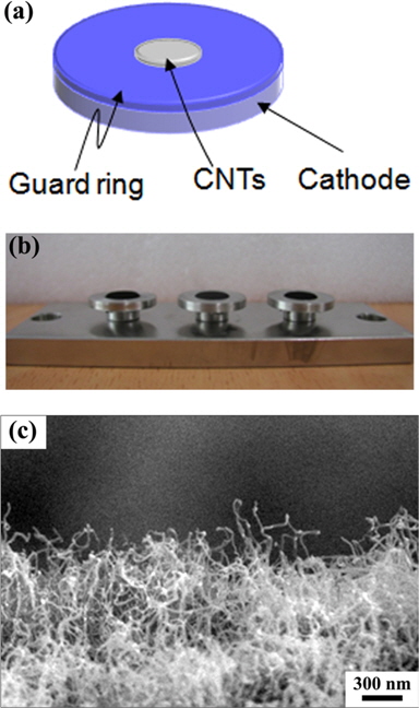
The fabrication procedure of the filtration-taping method is as follows. A uniform CNT film was formed onto a filter membrane using a vacuum ambient to filter a suspension of highly-dispersed CNTs[11,12]. Then, the CNT film was transferred to one side of a double-sided conductive tape (MAINELECOM, Ltd., the surface resistance is less than 4 mΩ/mm2) by pressing the membrane facing down on the tape. A circular disk with dimensions of 5 mm in diameter and 1 mm in thickness was attached onto the center of a stainless steel plate to form the cathode. The edge of the circular disk was ground to avoid edge emission [13]. Then, the conductive adhesive tape with CNT film faced up was set on the protruded circular disk. Finally, a 0.5 mm-thick stainless steel guard ring with a hole of 5mm diameter pierced in the center was put on, only exposing CNTs in the center region to act as the emitter, as shown in Fig. 1a. Fig. 1b shows three real CNT field emitters using the filtration-taping method, indicating a very simple but efficient technique.
It is worth noting that our emitter fabrication technique can be applicable to all types of CNT materials, including single-walled CNTs (SWCNTs), double-walled CNTs (DWCNTs), thick and thin multi-walled CNTs (MWCNTs). Since the same fabrication technique can be used for various CNT materials freely, it is possible for us to compare the performance of various types of CNT materials exactly. In this work, thin-MWCNTs were used because they can possess the merits of both SWCNTs (DWCNTs) and thick-MWCNTs due to their several concentric graphene layers. The morphology of the thin-MWCNT field emitter was characterized by scanning electronic microscopy (SEM, Hitachi, S-4700) and is shown in Fig. 1c. It can be seen that there are numerous vertically-aligned CNTs protruding from the substrate surface. It is well known that the vertically aligned CNTs can exhibit a better field emission performance than the randomly-oriented CNTs [6]. This is an important feature of the filtration-taping method. However, other methods, such as spraying, electrophoresis, and screen-printing, usually obtain randomly-oriented CNTs. Most of the CNTs are lying down, and hence, only a few protruding CNTs can participate in the field emission [14,15]. Accordingly, the special post-treatments, like soft rubber rolling, laser treatment, electrical annealing, thermal oxidation, argon irradiation, ultraviolet laser ablation, and adhesive taping, are needed to activate the randomly-oriented CNT emitters or remove some possible contamination [15-21]. But for the filtration-taping technique, CNTs are aligned during a transfer procedure when we separate the CNT film from the filter membrane. As a result, the filtration-taping technique demonstrates a simple and efficient method to fabricate the CNT emitters with excellent field emission properties.
The screen-printing and spraying methods are typically used to fabricate CNT emitters. In this work, we compared the field emission properties from the thin-MWCNT emitters using the three different fabrication techniques. The field emission measurement was performed using a planar diode configuration in a vacuum chamber at a pressure of 2 × 10⁻⁷ torr. The anode was a stainless steel plate. The gap between the cathode and the anode was adjusted to 400 μm. The same amount of thin-MWCNTs was used to obtain the field emitters.
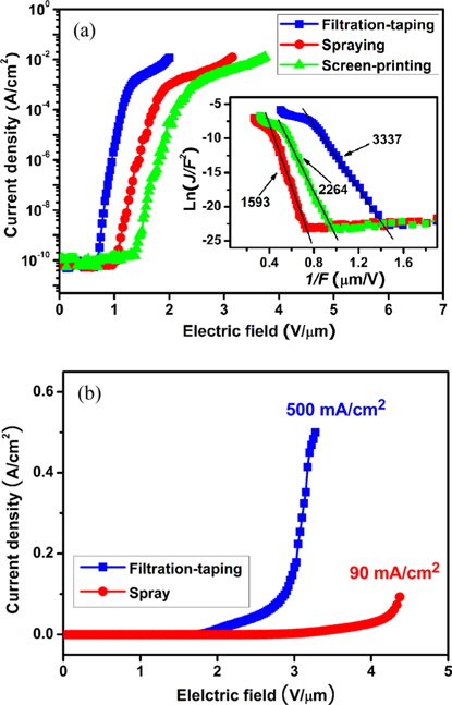
The field emission characteristics from thin-MWCNT emitters fabricated by filtration-taping, screen-printing, and spraying methods are shown in Fig. 2a. The CNT emitter fabricated by the filtration-taping method demonstrates the best field emission performance: the lowest turn-on electric field of 0.88 V/ μm at an emission current density of 0.1 A/cm2 and a threshold electric field of 1.98 V/μm at an emission current density of 1 mA/cm2, and the largest field enhancement factor of 3337. The achieved field emission performance is much higher than those of the previous results [8,22-24]. We consider that the largest field enhancement factor also confirms the vertical alignment of CNTs in the filtration-taping field emitter. In addition, a very high emission current density can be obtained using the filtration-taping method. As shown in Fig. 2b, an emission current density of 500 mA/cm2 is obtained at the applied electric field of 3.28 V/μm from a 5 mm-diameter CNT emitter with a gap of 400 μm. The higher emission current density can be achieved if the higher power supply is available. However, we can only obtain the emission current density of 90 mA/cm2 from the CNT emitter using the typical spraying technique. We attribute the excellent performance of the high emission current from the CNT emitter fabricated by the filtration-taping technique to the following advantages of the filtration-taping method: the high density of emission sites at the CNT emitter, the good electrical contact, the strong mechanical adhesion between CNTs and the cathode, and the low degradation of CNT tips due to the organic-free process. In addition, during the field emission measurement, arcing was usually observed under a high electric field from the CNT emitters fabricated by the screen-printing or the spraying methods whereas it was very rare from the CNT emitters fabricated by the filtration-taping method.
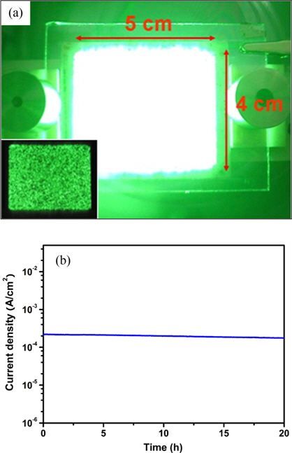
A bright image of electron emission pattern observed from a rectangular thin-MWCNT emitter with a large size of 5 × 4 cm2 is shown in Fig. 3a. The electron emission pattern was investigated using a phosphor-coated conducting indium tin oxide (ITO) glass as the anode. The gap and the applied voltage between the cathode and the anode were 3 mm and 3600 V, respectively. The thin-MWCNT emitter shows a uniform emission pattern and a high density of emission sites across the whole emitter region of 5 × 4 cm2. The dark image in the left bottom inset of Fig. 3a also confirms the uniform emission sites of the large size field emitter. The field emission stability is also a very important parameter for the practical application of the CNT field emitters. We evaluated the emission stability of the large size thin-MWCNT emitter. The initial emission current density was set at 0.18 mA/cm2. The thin-MWCNT emitter shows a very stable emission behavior with only 12.8% current degradation after 20 h, as shown in Fig. 3b, indicating that the filtration-taping method can provide excellent emission stability. Due to the degradation of the ITO glass, we also investigated the field emission stability using a 5mm-diameter emitter and a stainless steel plate as the anode and accordingly obtained an excellent stability with 20% current degradation for 20 h from an initial emission current density of 1 mA/cm2, which is a very severe acceleration lifetime test condition. We attribute the remarkable field emission stability to other good features of the filtration-taping method, i.e. the high mechanical adhesion between CNTs and the cathode and no contamination of CNT tips from harmful organic materials by adapting the organic-free process. Higher mechanical adhesion can permit CNT emitters sustainable on the cathode under the higher applied electric field so as to avoid being pulled out. In addition, the out-gassing from the organic materials is one of the main reasons for CNT degradation and vacuum deterioration, resulting in degradation of emission performance. For the conventional screen-printing method, some organic vehicles are used to fabricate CNT emitters, and they exist partially at the CNT emitters after removing the organic materials. Therefore, at the high electric field region, the ion bombardment of residual gases, which originate from the organic materials can destroy or modify the structure of CNT emitters, consequently reducing the emission current and stability [8]. However, the filtration-taping technique is an organic-free process so that the damage of the CNT emitters can be effectively avoided or alleviated.
In summary, we demonstrated a simple but efficient fabrication method for CNT emitters known as the filtration-taping technique. The following advanced field emission properties could be achieved from the filtration-taping CNT emitters: a low turn-on field of 0.88 V/m, a low threshold filed of 1.98 V/μm, a high emission current density of 500 mA/cm2, and good stability. We attribute the excellent field emission performance to the organic-free process and the simple contact-transfer process, which are the newly designed filtration-taping method. We strongly suggest that the filtration-taping technique is an effective way to realize low-cost, large-size, and high-performance CNT emitters.