Photovoltaic (PV) ribbon is widely used as an electric wire to form a connection between cells in a PV module [1-3]. PV ribbons are generally classified into two types: interconnector and bus-bar ribbons [1-3]. In order to enhance the adhesion between the ribbon and cell [4-11], Cu wire is first fabricated in a ribbon shape by rolling Cu wire. Next, PV ribbon is fabricated by melt plating Sn-Pb solders onto the internal Cu ribbon [12-18]. Recently, low-cost PV ribbons are in great demand because of the widespread need for PV modules [19-21].
The aim of this research is to study a new design of PV ribbon that can decrease the use of Sn-Pb solder. Generally, one side of the PV ribbon, especially in the bus-bar type, is being used as for the contact area with cells in PV modules. We suggest a new ribbon's design where the Cu wire's cross-section is a semi-ellipse. The semi-ellipse ribbons can decrease the use of Sn-Pb solder to 64% and increase the photovoltaic efficiency, by reducing the contact area between the ribbon and cell, to 80%. We also see an improvement in reflectivity on the curved surface.
Cu wire samples with different cross-section shapes were fabricated. Cu wires with a diameter of 1.9 mm were used for the PV ribbon samples. Each Cu wire was polished to have a different cross-section shape by fixing it to a self-made sample holder. Next, we fabricated PV ribbon samples, with different cross-section shapes, by melt plating with Sn-Pb solder. The composition of the Sn-Pb solder was Sn60-Pb40 (wt%) and the temperature of melt plating was 250℃. First, each Cu wire was coated with flux, and then plated with liquid Sn-Pb solder. The plating speed was 5.0 mm/sec.
Each sample was prepared for scanning electron microscope (SEM) measurement by being fixed using instantaneous adhesive with a self-made sample holder. Since Sn-Pb solder is very soft, the cross-sections of the SEM samples were precisely polished. The morphologies of the Cu wires and PV ribbons with different cross-section shape were then investigated by SEM. Especially, we minutely observed the thickness and shape of the Sn-Pb solder on the PV ribbons with different cross-section shapes.
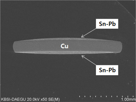
Figure 1 shows the SEM micrograph of the cross-section of the PV ribbon that is currently in widespread use. We can see from the figure the ribbon nature of the PV wire. In order to enhance the adhesion between the ribbon and cell, Cu wire with a 1.9 mm diameter was firstly elongated until it had a diameter of 1.0 mm, then it was rolled into 0.2 mm thick ribbon with a width of 2.0 mm. As shown in Fig. 1, the thickness of the Sn-Pb solder on the flat Cu surface is thicker, than that on a curved Cu surface at the edge. Also, the contact angle of the Sn-Pb solder on the flat Cu surface was observed to be lower than 90°, considering the crosssection shape of the Sn-Pb layer [22,23].
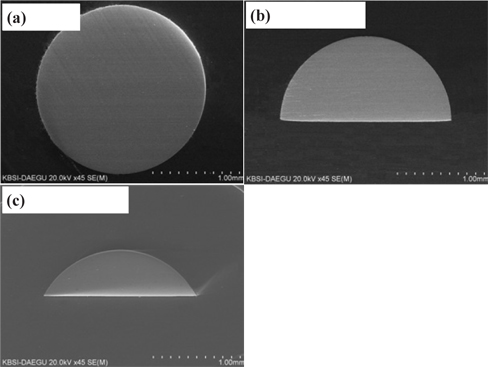
The aim of this research is to find a new design of PV ribbon that can decrease the use of Sn-Pb solder. Figure 2 shows the SEM micrographs of Cu wire with different cross-section shapes. Figure 2(a) shows Cu wire whose cross-section shape is a circle. The surface of the Cu wire is composed of only curved surface. Figure 2(b) shows Cu wire whose cross-section shape is a semicircle. The surface of the Cu wire is composed of a flat and a curved surface. Considering application, Fig. 2(c) shows Cu wire whose cross-section shape is a semi-ellipse. The surface of the Cu wire is also composed of flat and curved surfaces.
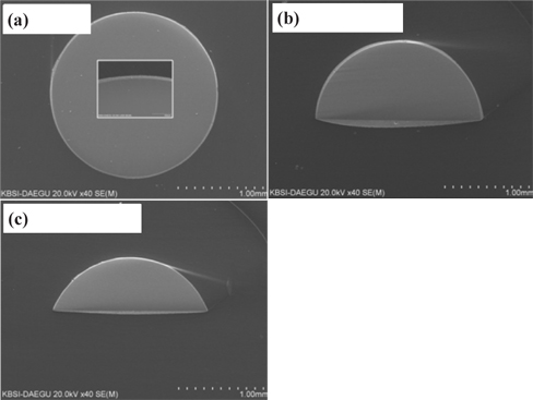
Figure 3 shows the SEM micrographs of PV ribbon with different cross-section shapes to study the plating properties of the Sn-Pb solder. The composition of the Sn-Pb solder was Sn60-Pb40(wt%). Figure 3(a) shows PV ribbon whose cross-section shape is a circle. The surface of the Cu wire is composed of only a curved surface. The inset more clearly displays the layer of Sn-Pb solder under higher magnification. The layer of Sn-Pb solder was plated thinly and uniformly around the whole wire. Figure 3(b) shows the PV ribbon whose cross-section shape is a semi-circle. The surface of the Cu wire is composed of flat and curved surfaces. The layer of Sn-Pb solder was plated relatively thickly on the flat Cu surface, compared to that on the curved Cu surface. The thickness of the Sn-Pb solder on the curved surface was very similar to seen in Fig. 3(a) with the circular wire.
Figure 3(c) shows the PV ribbon whose cross-section shape is a semi-ellipse. The surface of the Cu wire is also composed of a flat and a curved surface. Indicating a similar tendency to Fig. 3(b) with the semi-circular wire, the layer of Sn-Pb solder is plated relatively thickly on the flat Cu surfaces, compared to curved Cu surfaces. These results indicate that Sn-Pb solder plates more thickly on flat Cu surfaces, while it plates more thinly on curved Cu surfaces, regardless of the Cu cross-section's shape.
The mean thickness of Sn-Pb solder was 13.7
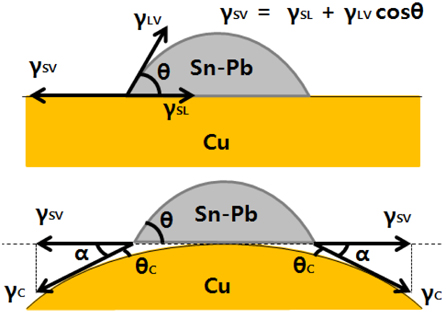
Figure 4 is a schematic that illustrates the different plating properties of a liquid Sn-Pb solder drops on flat and curved Cu surfaces. On the flat Cu surface, Fig. 4(a) illustrates the liquid solder drop, having a contact angle of less than 90° [10,11]. The schematic of the liquid Sn-Pb solder drop also shows the equilibrium state in Young's equation (γsv = γsl + γlv·cosθ) [24-28]. In the meanwhile, on the curved Cu surface with a semi-ellipse shape, Fig. 4(b) is a schematic of a liquid Sn-Pb solder drop. The contact angle on the curved Cu surface (θc) becomes geometrically smaller than that on the flat Cu surface (θ). Also, the surface energy of the curved Cu surface (γc) becomes geometrically bigger than that of the flat Cu surface (γsv). Therefore, the liquid Sn-Pb solder on the curved Cu surface is more thinly plated, because of the pulling from both sides with increased surface energy (γc).
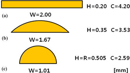
The contact area between the ribbon and cell is important for enhancing PV efficiency because PV ribbons block sunlight [29,30]. Figure 5 shows a comparison of cross-section shape and size of Cu wires with the same cross-section area of 0.40 mm2. Figure 5(a) shows a rectangular shape, where the width is 2.00 mm, the height is 0.20 mm, and the circumference is 4.20 mm, similar to that of a conventional ribbon. Figure 5(b) shows a semi-ellipse shape, where the width is 1.67 mm, the height is 0.35 mm, and the circumference is 3.53 mm at an arc angle of 90°. Therefore, the width of the Cu wire decreased to about 84%, compared to the rectangular shape, thereby contributing to the enhancement of PV efficiency. Figure 5(c) shows a semi-circular shape, where the width is 1.01 mm, the height (radius) is 0.505 mm, and the circumference is 2.59 mm. Therefore, the width of Cu wire has decreased to about 50%, compared to the rectangular shape. Considering the increase in contact resistance due to the decrease of contact area [31], we carefully calculated that the decrease in light blocking area by the Cu shape is significant. From these results, we suggest that semi-ellipse ribbons can decrease the contact area with a cell to about 84%, thereby contributing to the enhancement of PV efficiency, compared to that of conventional ribbon. The semi-ellipse ribbons can also increase the photovoltaic efficiency by improving reflectivity on curved Cu surfaces, compared to conventional ribbon with a flat Cu surface.
Our study looked at the plating properties of Sn-Pb solder according to the shape of Cu wire's cross-sections for photovoltaic ribbon. Regardless of the shape of the Cu wire's cross-section, the mean thickness of the Sn-Pb solder was 41.5