A new CMOS analog design methodology using an independently optimized self-cascode (SC) is proposed. This idea is based on the concept of the dual-workfunction-gate MOSFETs, which are equivalent to SC structures. The channel length of the source-side MOSFET is optimized, to give higher transconductance (gm) and output resistance (rout). The highest gm and rout of the SC structures are obtained by independently optimizing the channel length ratio of the SC MOSFETs, which is a critical design parameter. An operational amplifier (OPAMP) with the proposed design methodology using a standard digital 0.18-μm CMOS technology was designed and fabricated, to provide better performance. Independently gm and rout optimized SC MOSFETs were used in the differential input and output stages, respectively. The measured DC gain of the fabricated OPAMP with the proposed design methodology was approximately 18 dB higher, than that of the conventional OPAMP.
Modern CMOS technologies continue to scale down to the nanometer regime, and the power supply has also reduced to an ultra-low voltage of 0.5 V. Although this evolution in CMOS technology is suitable for digital circuitry, this is not so beneficial for analog circuits [1-4]. Excessively-scaled device dimensions show reduced output resistance, due to channel length modulation (CLM). Moreover, enhancing the analog circuit performance using the general analog circuit design methodology, such as the use of long channel devices and conventional cascode configurations, is difficult, due to threshold voltages (VTH) and output swing limitations.
The self-cascode (SC) structure is widely used to reduce the CLM effect, and is utilized in the design of a low-voltage operational transconductance amplifier (OTA), which shows high DC gain and output voltage swing [4-6]. On the other hand, the large channel width and length (W/L) ratio of two MOSFETs with a SC structure is one of its disadvantages. Asymmetric-VTH SC structures using low-VTH MOSFET have been proposed [7]. This approach requires a lower W/L ratio, but additional fabrication processing steps are unavoidable. Currently, an asymmetric-VTH SC structure can be easily implemented, using forward bodybiasing techniques in a triple-well technology, or silicon-oninsulator (SOI) technology [8,9]. The SC structure can also be used for an indirect compensation technique, for high speed operational amplifier (OPAMP) [8,10]. The dual-workfunctiongate (DWFG) MOSFET is a newly introduced transistor with an asymmetrically-doped poly-silicon gate, to increase the output resistance (rout) and transconductance (gm) [11]. The length of the source-side gate with a higher workfunction is an important variable for optimizing rout and gm. Surprisingly, the DWFG MOSFET is a similar concept to the SC structure, and can be applied to analog circuit design, but this technique requires complicated processing steps.
This paper proposes a new CMOS analog circuit design methodology, using SC structures and the DWFG concept. In the proposed method, the channel length of the SC structure in a standard digital CMOS technology is separately optimized for a higher gm and rout. Using this optimizing method, a two-stage OPAMP with higher gain was fabricated, and measured to verify the proposed idea. A 0.18-μm standard triple-well CMOS technology was used to both simulate, and fabricate the OPAMP, using the proposed design method.
This paper is organized as follows. Section 2 introduces the proposed analog design methodology, and its application to the design of a two-stage OPAMP. Section 3 presents the experimental results of a comparative study of the SC and equivalent single MOSFET. The measured performances of the fabricated twostage OPAMP using the proposed design methodology are also summarized. Finally, the conclusions are reported in section 4.
This section describes the channel length optimization of the SC structures with respect to gm and rout, as well as the application of the proposed design methodology to the design of a twostage OPAMP.
2.1 Analog design methodology using optimized self-cascode
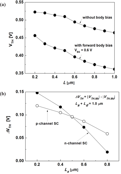
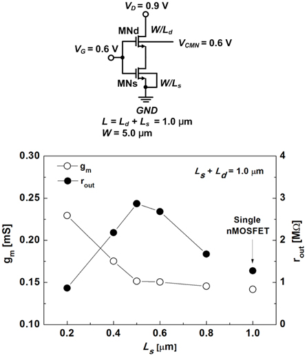
Figure 1 shows the simulated gm and rout characteristics of the n-channel SC structure (nSC). The n-channel MOSFETs (nMOSFETs) of MNd and MNs are connected in series, and a forward body-bias for MNd, which is insufficient to turn on the parasitic body-source diode, is applied to reduce VTH, without using a low-VTH MOSFET. A forward body-bias is not possible for the conventional body grounded nMOSFET. Therefore, triple-well or SOI CMOS technology is required. A deep n-well was used to allow the body of the nMOSFET MNd to be slightly forwardbiased. With VCMN = 0.6 V, the VTH of MNd is reduced by approximately 0.1 V. The total channel length (L = Ls + Ld) is 1.0 μm, and a channel width of 5.0 μm is used for both MNd and MNs. The SC structure is a well-known circuit configuration for lowvoltage analog circuit design [4-7]. The nMOSFET MNs normally operates in the triode regime, and MNd operates in the saturation regime. The effective rout of the nSC is approximately the triode resistance of MNs multiplied by the intrinsic gain of MNd (rout.eff ≈ gm.MNd · rout.MNd · rout.MNs). Therefore, if the triode resistance of MNs increases, the effective rout of nSC can be enhanced. If the VTH of MNd is reduced, the drain-source voltage VDS of MNs increases, and the operation of MNs moves from the triode to the saturation regime. Consequently, the effective rout of nSC can be maximized, when VDS of MNs approaches the overdrive voltage (VOV = VGS - VTH) of MNs. The condition of Eq. (1) should be satisfied by forward-biasing the body of MNd to give the highest rout and output voltage swing [7].

Figure 1 shows that both gm and rout are strong functions of the channel length of the source-side MOSFET MNs (Ls). The nSC with Ls = 0.5 μm shows the highest rout characteristics, compared to the equivalent single nMOSFET with L = 1.0 μm. The characteristics of gm are different from those of rout. The gm of the nSC with Ls = 0.5 μm is similar to that of the single nMOSFET with L = 1.0 μm, but when Ls is reduced below 0.5 μm, then gm of the nSC begins to improve. The reason is as follows: the effective gm of the nSC is dominated by the gm of the source-side transistor MNs. Hence, a more enhanced gm of the nSC with shorter Ls is observed. From Fig. 1, the nSC with Ls = 0.2 μm shows the highest gm.
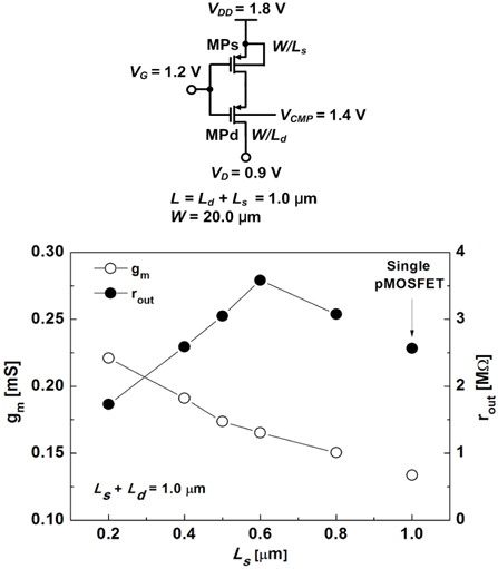
Figure 2 shows the simulated gm and rout characteristics of the p-channel SC structure (pSC), as a function of Ls. A forward body-bias for p-channel MOSFET (pMOSFET) MPd is also applied to reduce |VTH|. Therefore, pMOSFET with a separated nwell was used for MPd. With VCMP = 1.4 V, |VTH| of MPd is reduced by approximately 0.1 V. The total channel length (L = Ls + Ld) is 1.0 μm, and a channel width of 20.0 μm is used for both MPd and MPs. The pSC with Ls = 0.6 μm shows the highest rout characteristics, compared to the equivalent single pMOSFET (L = 1.0 μm). On the other hand, the pSC with Ls = 0.2 μm shows the highest gm.
From Figs. 1 and 2, the shorter Ls of the nSC and pSC shows more enhanced gm characteristics than the single n and pMOSFETs, because the source-side MOSFETs MNs and MPs determine the effective gm of the SC structures. On the other hand, the largest rout characteristics of the nSC are observed when the source and drain-side MOSFETs of the nSC have identical length (Ls = Ld). If the channel length of the source-side MOSFET Ls is less than 0.5 μm, rout.MNs decreases. Therefore, the effective rout of nSC is reduced. If Ls > 0.5 μm, the VTH reduction is no longer possible, due to the reverse short channel effect (RSCE) of the nMOSFET, as shown in Fig. 3 (a). In other words, nSC cannot satisfy the previously mentioned condition Eq. (1) to achieve a higher effective rout. Another factor is that rout.MNd decreases, due to the short channel length. Therefore, Ls = Ld shows the largest rout of nSC. Fig. 3 (b) shows the VTH difference between the source and drain-side MOSFETs (ΔVTH) of the nSC and pSC structures. The pMOSFET also has RSCE, but it is less severe than that of nMOSFET, i.e. the ΔVTH of the pSC is less sensitive than that of the nSC. The effective rout tendency of the SC structure is dependent on the device characteristics in the adopted CMOS technologies. Figures. 1 and 2 show that the channel length of the source-side MOSFET (Ls) is a critical parameter for the gm and rout optimization of SC structures. Figs. 1 and 2 also show that the SC structures have different optimized Ls values for gm and rout, i.e., they should be independently optimized.
2.2 Application to the design of a two-stage OPAMPs
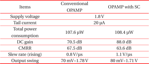
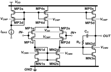
The OPAMP is a fundamental building block of many analog and mixed-signal systems. The design of the OPAMPs continues to pose a challenge, as the supply voltage and device channel length scale down with each generation of CMOS technology. The gm or rout optimized SC structures described in the previous subsection are applied to the two-stage OPAMP, as shown in Fig. 4. To enhance the performance of OPAMP, the gm optimized SC MOSFETs (Ls = 0.2 μm) are used for the differential input pairs of the pSC MP1-MP2, and the rout optimized pSC MOSFETs (Ls = 0.6 μm) are used in the current mirror MP3-MP5. In addition, the rout optimized nSC MOSFETs (Ls = 0.5 μm) are used in the active load MN1-MN2 and 2nd stage common-source amplifier MN3. The supply voltage (VDD) is 1.8 V. The forward body-bias voltages VCMP and VCMN are 1.4 V and 0.6 V, respectively. The tail current of the differential input stage is 20 μA.
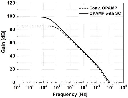
Figure 5 shows the simulated frequency response of both the conventional OPAMP with the equivalent single MOSFETs, and the OPAMP with the independently optimized SC MOSFETs. The DC gain of OPAMP with the optimized SC structures is 99 dB, which is 14 dB higher than that of the conventional OPAMP. The use of the gm optimized pSC in the differential input stage helps achieve a higher unity-gain frequency fT. The unity-gain frequency of OPAMP with the optimized SC is 9.85 MHz, which is 2 MHz higher than the 7.82 MHz of the conventional OPAMP.
The input-referred noise of the OPAMP can be reduced, by maximizing the transconductance of the differential input pairs for a given bias current [10]. The input-referred thermal noise voltage level of the proposed OPAMP is 18.9 nV/(Hz)1/2, which is 26% lower than that of the conventional OPAMP with the single MOSFETs.
The common-mode rejection ratio (CMRR), and the powersupply rejection ratio (PSRR) of the differential pairs, are proportional to the output resistance of the tail current source. Therefore, the rout optimized pSC MP4 in Fig. 4 helps enhance the CMRR and PSRR of the OPAMP. The PSRR of OPAMP with the optimized SC is largely improved, as shown in the simulated performance summary in Table 1. On the other hand, the CMRR of the OPAMP with the optimized SC is similar to that of the conventional OPAMP, because of the enhanced common-mode gain of the 2nd stage.
[Table1.] Simulated performance of the two-stage OPAMPs.
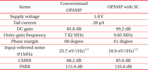
Simulated performance of the two-stage OPAMPs.
To confirm the proposed design methodology, the OPAMP with the optimized SC structures, and conventional OPAMP with the single MOSFETs were fabricated, using a 0.18-μm standard digital CMOS technology. The electrical characteristics of the SC differential input transistors, SC current mirrors, unity-gain buffer using the proposed OPAMP, and finally performance parameters of the fabricated OPAMP were measured.
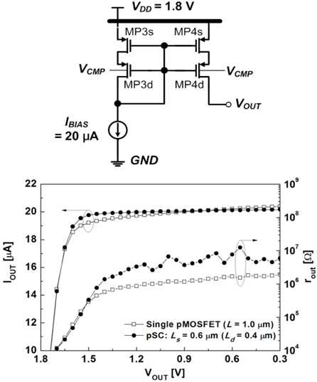
Figure 6 shows the measured output current (IOUT) and rout characteristics of the current mirror, with the pSC MOSFETs and single pMOSFETs. The overall channel length and width of the MOSFETs were 1.0 μm and 20.0 μm, respectively, and the channel length of the source-side MOSFET was 0.6 μm. The applied bias current was 20 μA. The semiconductor parameter analyzer (Agilent 4156C) was used for the measurements. The measured rout of the conventional current mirror was 1.1 MΩ at VOUT = 0.9 V, but the measured rout of the pSC current mirror was approximately three times higher than that of the conventional mirror. The enhanced output resistance of the pSC current mirror confirmed the reduced CLM of the MOSFETs.
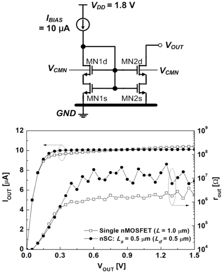
Figure 7 shows the measured IOUT and rout characteristics of the nSC current mirror. The channel length Ls of the source-side MOSFET was 0.5 μm, and the channel width of all transistors was 5.0 μm. The applied bias current was 10 μA. The measured rout of the conventional current mirror was 1.5 MΩ at VOUT = 0.9 V. On the other hand, the nSC current mirror showed approximately four-fold improvement in rout. The improvement in rout of the nSC current mirror is better than that of the pSC.
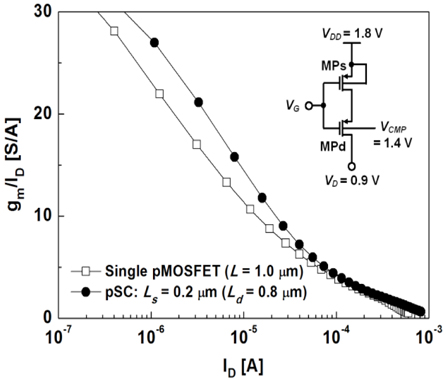
Figure 8 shows the measured transconductance generation efficiency (gm/ID) of the gm optimized pSC MOSFETs (Ls = 0.2 μm) at VSD = 0.9 V. The channel width of all transistors was 20.0 μm. Compared to the conventional single pMOSFET, the pSC MOSTFET showed approximately 30% improvement in the gm/ID at a drain current ID = 10 μA.
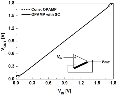
Figure 9 shows the measured DC transfer characteristics of the unity-gain buffer, using the proposed OPAMP with the optimized SC MOSFETs. The applied input voltage VIN varied from 0 V to 1.8 V. The measured output voltage followed the input voltage over the entire range. The output voltage range of the OPAMP with the optimized SC structures ranged from 80 mV to 1.71 V.
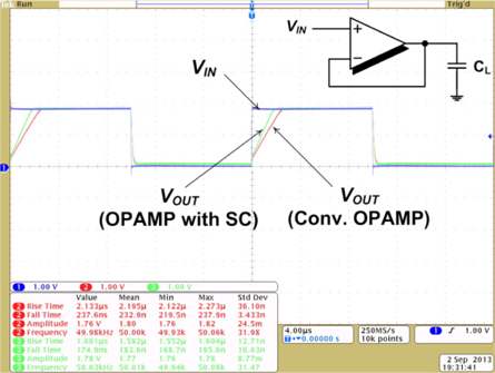
Figure 10 shows the measured large signal step response of the unity-gain buffer using the proposed OPAMP with the optimized SC MOSFETs. The load capacitor CL was 15 pF. The applied step input voltage and frequency were 1.8 V and 50 kHz, respectively. The maximum rising slew rate of the proposed OPAMP was similar to the ratio of the charging current of MP5 and load capacitor (≈ IMP5/CL) [12]. The rising slew rate of the proposed OPAMP was 1.1 V/μs, which was a 33% improvement, compared to the conventional OPAMP with the single MOSFETs. Although the charging current of MP5 was identical (20 μA) for both the conventional and proposed OPAMPs, the rising slew rate of the proposed OPAMP could be improved due to the reduced CLM, as shown in Fig. 6.
The DC gains of the fabricated OPAMPs were measured, using a simple measurement technique with a servo loop and auxiliary OPAMP (μA741) [13]. The measured DC gain of the OPAMP using the optimized SC was 88.0 dB, which was approximately 18 dB higher than that of the conventional OPAMP. The enhanced gm and rout of the SC structures resulted in a higher DC gain of the OPAMP. Table 2 lists the measured performance data of the proposed OPAMP, along with that of the optimized SC and the conventional OPAMP.
[Table 2.] Measured performance of the fabricated OPAMPs.

Measured performance of the fabricated OPAMPs.
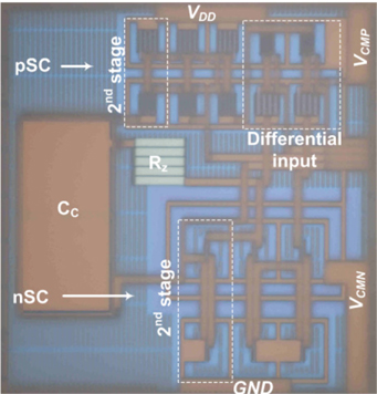
Figure 11 shows the micrograph of the proposed OPAMP with optimized SC structures, which was fabricated in a standard 0.18-μm triple-well CMOS process. The chip area was 80 μm × 86 μm.
This paper reports a new analog circuit design approach, using SC structures based on the concept of dual-workfunctiongate devices. Both the transconductance and output resistance were influenced by the channel length ratio of the SC MOSFETs. Optimizing the channel length ratio of the SC structure, the highest transconductance and output resistance SC MOSFETs were obtained and utilized in the input differential stages and output stages of the operational amplifier, respectively, to obtain better performance. A two-stage OPAMP using the proposed SC MOSFETs was designed and fabricated. The measured DC gain of the fabricated OPAMP using the proposed SC MOSFETs was approximately 18 dB higher, than that of the conventional OPAMP. The proposed design methodology is a promising solution for lowvoltage analog circuit design, particularly in nano-scale CMOS technologies.