A novel memory is reported, in which Ge2Sb2Te5 (GST) has been used as a floating gate. The threshold voltage was shifted due to the phase transition of the GST layer, and the hysteretic behavior is opposite to that arising from charge trapping. Finite Element Modeling (FEM) was adapted, and a new simulation program was developed using c-interpreter, in order to analyze the small shift of threshold voltage. The results show that GST undergoes a partial phase transformation during the process of RESET or SET operation. A large VTH shift was observed when the thickness of the GST layer was scaled down from 50 nm to 25 nm. The novel 1 transistor PCM (1TPCM) can achieve a faster write time, maintaining a smaller cell size.
The impressive growth of the portable systems market in the last decade has attracted the attention of the semiconductor industry toward non-volatile memory (NVM) technologies. Table 1 shows the respective memory characteristics by the international technology roadmap for semiconductors (ITRS) [1,2].
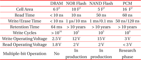
Device characteristics of DRAM, Flash, and PCM [1]. Information is gathered from the ITRS, and does not represent the best-of-breed for specific product and research advances [2].
NOR and NAND flash - charge trapping/detrapping within an insulator stack - are integrated into a field effect transistor [3], leading to compact designs with 1 transistor. Generally, in ultra-small devices, the injection phenomena and the energetic interactions affect the reliability, endurance, and operating characteristics (e.g. slowing down of the write/erase time).
Phase change memory (PCM) uses the conductivity change arising from a phase change between amorphous and crystalline phases [2,4], and typically employs an access element (a diode, FET or a bipolar transistor), in series. PCM exhibits good write/erase time. However, this kind of setup encounters the following problems: power, scaling issue from surface effects and the requirement of too much space for the two elements.
Previously, we proposed and fabricated a 1 transistor PCM (called 1TPCM) with Ge2Sb2Te5 (GST) as a floating gate [5]. The phase change in the GST material occurs by the heat developed in the device as a result of current flow.
Additionally, a shift of threshold voltage was realized due to changes in conductivity and permittivity of the material, arising out of the amorphous and crystalline phase transformation in the gate dielectric layer.
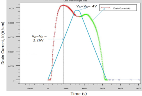
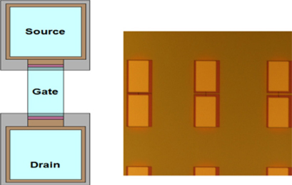
Our novel 1TPCM had a small cell area comparable with a DRAM, and operated at a low write/erase voltage and fast write/ erase time (Fig. 1).
However, the measured results showed that the threshold voltage (VTH) shift was smaller than the expected value [5]. The 1TPCM was designed using simple mathematical calculations before the simulation modeling was even developed.
In the current work, Finite Element Modeling (FEM) was adapted, and a new simulation program was developed using c-interpreter, to analyze the observed small shift of the threshold voltage in 1TPCM.
2. STRUCTURE AND MODELING OF THE NOVEL 1TPCM
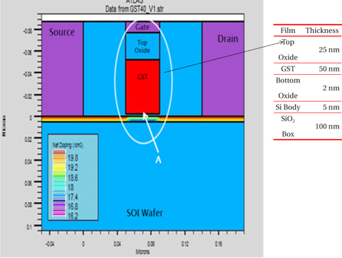
Figure 2 shows the thickness and structure of the 1TPCM that was used in the simulation. Basically, the MOSFET is fabricated on the silicon-on-insulator (SOI) substrate and the gate dielectric layer consisted of GST, which was in the middle of silicon dioxides. The temperature of the GST was measured at a point located at the middle of the x axis and the interface between the GST layer and bottom oxide of the y axis (A in Fig. 2).
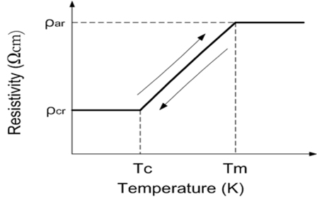
When a voltage was applied across the gate and the drain electrodes, the drain current generated heat (Joule’s heating) within the channel. On application of the RESET pulse, the temperature of the GST became larger than its melting temperature (Tm), leading to a phase change from the crystalline to the amorphous form. 1TPCM then indicated a high threshold voltage, which could be used as logic “1”. The SET pulse raised the temperature of GST higher than its recrystallization temperature (Tc), which was lower than Tm, and brought the VTH to a low state, which was named as logic “0”.
2.2 Finite element modeling and simulation
Equation 1 can be used to treat heat transfer by conduction mathematically.

where, ρ is the density, T is the temperature, C is the heat capacity, k is the thermal conductivity, t is the time, and Q is the heat flux [6].
The heat generated by Joule heating Q is given by
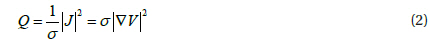
where, σ is the electric conductivity, J is the electric current density, and V is the electric potential.
Based on Silvaco’s TCAD tool, the FEM was adapted, and a new simulation program was developed, using the c-interpreter. Any changes in conductivity and permittivity values were investigated from the temperature change in the 1TPCM, especially in the GST region.
Appropriate programming was done to evaluate the changes in conductivity and permittivity values from the temperature change in GST and to obtain a thermal hysteresis curve as shown in Fig. 3, where,
Boundary conditions for temperature simulation are defined as 300 K at the bottom end of SOI substrate and top of the gate, source, and drain electrodes. The physical properties of the GST used in the simulation process are listed in Table 2.
[Table 2.] Physical properties of the materials used in simulation [6,7].
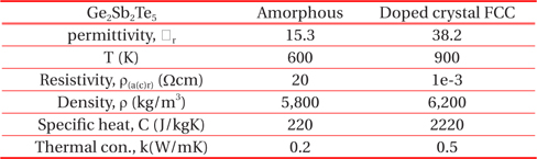
Physical properties of the materials used in simulation [6,7].
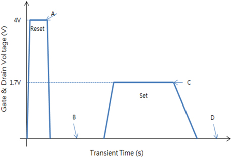
In order to define the RESET pulse condition, a voltage pulse was simultaneously applied at the gate and drain electrodes. The pulse ramped up from 0 V to 4 V in 30 ns, stayed at 4 V for 5 ns, then finally ramped down to 0 V in 30 ns (Fig. 4).
The maximum drain current of 1.03 mA, was realized in 17 ns, when both the gate voltage (VG) and the drain voltage (VD) were 2.26 V. Any further increase in the voltage (up to 4 V) led to a gradual decrease in the drain current, which is probably caused due to a decrease in mobility and permittivity of GST. This behavior signifies a typical I-V sweep characteristic of PCM materials. However, on application of 4 V voltage, a faster write time of 4 ns was achieved, compared to the 17 ns in conventional PCM. Additionally, at the highest drain current, the temperature at point A in Fig. 2 became 979 K.
It was also found that the drain current continued to increase, when the voltage started to decrease from 4 V, until it reached the value of 3 V, after which the drain current started to decrease again. This is because recrystallization occurs in partial areas of the GST at a slow ramping down speed of 0.13 V/1 ns. The falling time of the RESET pulse must be short enough so as to not allow GST to be recrystallized. The operating conditions and the corresponding results are shown in Figs. 5 and 6 respectively.
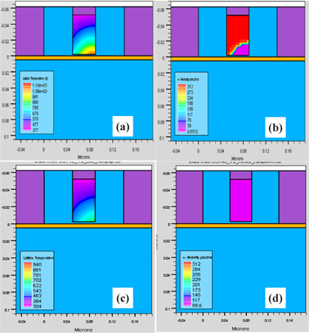
After a RESET pulse is applied to the 1TPCM at point A in Fig. 5, the temperature and mobility values are displayed in Figs. 6 (a) and 6 (b), respectively. The region whose temperature is above 900 K exhibited an amorphous mobility. Figure 6(c) indicates the temperature at point C in Fig. 5, which is the starting point of the decreasing SET pulse. The temperature of the amorphous region was 600~700 K. At this temperature recrystallization GST can occur. Finally, Fig. 6 (d) displays the change of amorphous mobility to the crystalline one, corresponding to the point D in Fig. 5.
It was found that the entire GST layer does not undergo a phase change at one time. This explains the very small shift in the threshold voltage in the previously reported device [5].
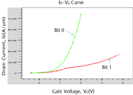
Furthermore, even an increase in the RESET pulse duration time up to 50 ns (not to exceed PCM write time) is not sufficient for any observable VTH shift. However, scaling down of the GST layer thickness from 50 nm to 25 nm and threshold voltages measured at points B (bit 1) and D (bit 0) in Fig. 5, show a VTH shift of 0.8 V at drain current of 1 μA/μm.
The 1TPCM cell has 1 transistor, a low RESET/SET voltage, a fast write/erase time, an acceptable amount of VTH shift, and a small cell so that it could be suitable for future production of NVM.
Adapting the Finite Element Modeling and using a simulation program developed with c-interpreter, the current research has reported a novel 1TPCM, which has the combined advantages of both a conventional PCM and a DRAM.
Using the simulation, it was possible to explain the shift in the threshold voltage of the previously reported 1TPCM. The partial phase change of the GST layer, during RESET/SET, was not able to induce a sufficient VTH shift. Scaling down of the GST layer thickness from 50 nm to 25 nm resulted in a VTH shift of 0.8 V and ID difference of 1 μA/μm between bit 1 and bit 0 at an applied read voltage of 1 V. Finally, the 1TPCM cell reported in this work has 1 transistor, a low RESET/SET voltage, a fast write/erase time, and a small cell, so that it could be suitable for future production of NVM.
It is expected that a more efficient 1TPCM would be possible, by using a material that shows a phase change at a temperature lower than that of GST.

![Device characteristics of DRAM, Flash, and PCM [1]. Information is gathered from the ITRS, and does not represent the best-of-breed for specific product and research advances [2].](http://oak.go.kr/repository/journal/13460/E1TEAO_2014_v15n1_37_t001.jpg)


![Physical properties of the materials used in simulation [6,7].](http://oak.go.kr/repository/journal/13460/E1TEAO_2014_v15n1_37_t002.jpg)