Highly integrated device demands more accurate CD (Critical Dimension) control, and high contrast PR (Photoresist) is needed for the exposure threshold effect [1,2], however, the reflectivity between substrate and PR becomes higher. Therefore, the CD swing curve was intensified, which was directly influenced by the change of PR thickness. The higher reflectivity also causes PR notching due to the pattern of sub-layer. An accurate CD control and bottom anti-reflective coating (BARC) can eliminate the reflectivity between substrate and PR [3,4]. In the current semiconductor manufacturing process, silicon oxynitride (SiON; SixOyNz) has been used as an inorganic BARC for metal pattern process of the above 0.18-μm-device, but the under 0.13-μm-device needs more elaborate CD control. Several conditions such as the thickness of PR, refractive index (n) and absorption coefficient (k) as well as metal stack as a sub-layer should be modified. In addition, standing wave was observed in PR profile after metal pattern process of 0.13-μm-device, which was caused by the unsuitability of BARC for 0.18-μm-device to the changed PR and sub-layer for 0.13-μm-device to lead the higher reflectivity. The reflectivity of BARC / PR interface is determined by three optical factors: the thickness, refractive index and absorption coefficient of BARC(SiON). In order to secure the deposition conditions of SiON film to produce a minimum reflectivity for inorganic BARC for 0.13-μm-device, the refractive index and absorption coefficient of SiON film were investigated by changing the ratio of SiH4/N2O gas flow as one of the most important process parameters. Because the reflectivity of BARC / PR interface could not be measured directly, it could be obtained through the computational simulation of reflectivity by changes of optical factors of BARC with a certain source of light, optical factors of PR and conditions of sub-layer. The optimum thickness, refractive index and absorption coefficient could be determined through the computational simulation to minimize the reflectivity with applying SiON film. The cross-sectional scanning electron microscopy (SEM) images of PR were analyzed to confirm the standing wave [1,3,5].
When light passes through media with different refractive indexes, light is reflected, absorbed or penetrated. Like this, the refractive indexes to exposure source are different in the air, PR and substrate, to produce reflection between interfaces and multipath ghosts in the PR layer. Light intensity is presented with as a function of the thickness of PR with a variation shape from minimum to maximum by the thickness of PR as a formula of d = λm / 2n0. Here, n0, λ and m are a refractive index of PR, an incident light and a positive integer, respectively. For PR with inevitably different thickness caused by some phenomena including step height accumulated in the same device, the relative amount of the exposed energy per volume unit in forming patterns depends on the changes of thickness to cause the difference in CD called as CD swing. At this time, PR profile shows a vertical curve named standing wave, which resulted from the light-energy coupling variations through the destructive and constructive interference caused by the PR thickness variation [5]. PR notching is defined as transforming PR pattern due to sideways reflection or light scattering following surface grain from the pattern of sublayer. All these phenomena were originated from the reflection of substrate / PR interface. Therefore, the control of reflectivity is essential for a precise CD control and the phenomena like CD swing, standing wave and PR notching, which can be reduced effectively by a decrease in reflectivity in the BARC / PR interface by applying BARC between substrate and PR. BARC can minimize the reflectivity of surface with the following two methods: one is the offset of phase shift by using the combination of refractive index and thickness [6-9]; the other is the absorption of film itself caused by absorption coefficient [6-9]. Assuming that a light is normally incident on a uniform and isotropic film, the reflectivity in the interface of BARC / PR can be expressed as follows:
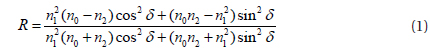
Where δ expresses the phase difference across the film, λ the wavelength of the light, n0 the refractive index of PR, n1 refractive index of BARC, and n2 refractive index of substrate. The reflectivity is minimized in formula (1) when path of light △ = λ / 2 (i.e., thickness t = λ / 4n). If the path of light to BARC / PR interface through BARC is (2m + 1)λ / 4n (m is a positive integer), the reflected light from BARC / PR interface has a phase shift by λ / 2 (180˚) with the light from the surface to be offset due to the destructive interference; this is called the phase shift cancellation. The other is light absorption of film itself. Absorbance (α) is related to absorption coefficient (k) and is presented with formula (2). Light intensity (I) is changed according to Lambert’s law when it passes a film vertically.

Where the absorbance and the optical transmittance (T) of a film are expressed as follows:


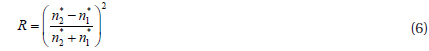
Therefore, the absorption of light, which was determined by k-value, is an exponential function by the thickness of t. Appropriate k-value must be selected because the higher absorption coefficient leads, the higher n2* in Fresnel’s equation; this calculates the reflectivity on the interface to the incident light as shown in formula (6), to increase in the reflectivity on the interface, although the higher absorption coefficient is considered to be optimum as an anti-reflection layer with the more absorption and the less penetration of light.
Where is referred to a complex refractive index ( n - ik ). In order to minimize the reflectivity of BARC / PR interface, the two principles of phase shift cancellation and absorption are represented as the superposition of graphs in which a sinusoidal graph is based on the refractive index and an exponential graph of light absorption is based on the absorption coefficient.
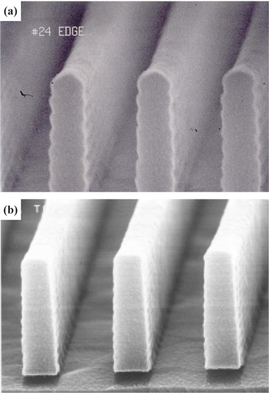
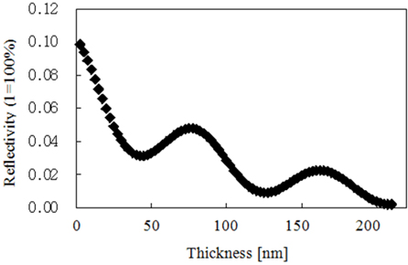
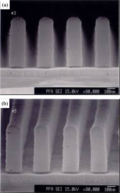
The semiconductor manufacturing process over 0.18-μmdevice used the SiON of the SiON 25.0 nm / silicon dioxide (SiO2) 5.0 nm structure in an inorganic BARC process. The SiON as BARC had the thickness of 25.0 nm, refractive index of 1.83 and absorption coefficient of 0.14 in the process over 0.18-μm-device. The SiO2 was utilized as a barrier layer in order not to provoke PR footing caused by the reaction between amine group (NH-) on the surface of SiON film and acid components of the PR for deep ultraviolet (UV) [10,11]. PR standing wave was observed when the above process conditions were directly applied to the manufacturing process for the 0.13-μmdevice as shown in Fig. 1(a), unlike the case for the PR profile of 0.18-μm-device which showed no standing wave as shown in Fig. 1(b). The PR and sub-layer for 0.13-μm-device were changed with the same optical factors of SiON film as shown in Table 1. Particularly, the process condition for 0.13-μm-device demanded more elaborate CD control so that the thickness of PR should decline to 610 nm; however, the thinnest thickness of the conventional PR (PEK111) used for 0.18-μm-device was 680 nm, so the PR for 0.13-μm-device was changed by UV135 which could be modified into the thinner thickness of 610 nm with the same or similar optical factors of PR. The BARC for the conventional 0.18-μm-device brought out the standing wave due to the inappropriateness of the shrink PR and sub-layer for 0.13-μm-device; this means that a more accurate control of BARC would be required for the reduced PR and sub-layer through the control of reflectivity. Therefore, the reflectivity of BARC / PR interface should be investigated and controlled even though the reflectivity of BARC / PR interface could not be measured directly by experiments. The algorithm of computational simulation was formulated for the stacked structures of isotropic materials. When the computational simulation of reflectivity of BARC / PR interface was performed under the current conditions of the BARC as shown in Fig. 2, the thickness above 100.0 nm of SiON was associated with approximately 2% of reflectivity to prevent the standing wave since the reflectivity of the conventional 25.0-nm-thick SiON was over 5% which had induced the standing wave. However, the thick SiON causes the process to be very hard to remove the BARC layer after PR pattern in metal etching process so that the thickness was not applicable. Therefore, the appropriate conditions for the BARC including thickness, refractive index and absorption coefficient should be improved.
[Table 1.] Process conditions for 0.18-μm-device and 0.13-μm-device
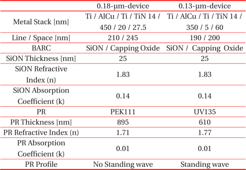
Process conditions for 0.18-μm-device and 0.13-μm-device
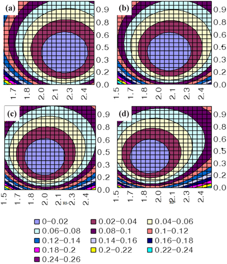
In order to find the appropriate conditions including thickness, refractive index and absorption coefficient of the SiON film as BARC for the PR and sub-metal layer of 0.13-μm-device, the computational simulation for the reflectivity of primary BARC / PR interface was performed. The thickness of SiON was limited in the range of 25.0 to 40.0 nm by considering the process margin for the metal etching process [12,13]. Figure 3 shows the results of computational simulation performed with thickness of 25.0, 30.0, 35.0 and 40.0 nm, refractive index of 1.5~2.5 and absorption coefficient of 0~10. According to the computational simulation results, the condition for minimizing the reflectivity corresponded to the absorption coefficient of approximately 0.4, which showed the thickness of 25.0 nm and refractive index of 2.2 in this condition; however, the thicker value was associated with the lower refractive index to reduce the reflectivity with an inverse proportion. Therefore, the optimized condition of SiON film as BARC with the minimum reflectivity should be chosen at the absorption coefficient of approximately 0.4. The refractive index had a definite value at the absorption coefficient of 0.4 because the refractive index and the absorption coefficient change with a consistent tendency. The thickness to minimize the reflectivity should be determined with the certain refractive index at the absorption coefficient of 0.4. The thickness of the inorganic BARC SiON film was controlled by the time for film preparation. The refractive index and the absorption coefficient could be changed by the gas flow ratio of SiH4 and N2O as reactants in forming the film
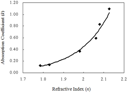
Experimental study was carried out by using the conventional plasma-enhanced chemical vapor deposition (PECVD, AMAT, Centura5200 DxZ). Table 2 shows the refractive index of SiON film as a function of gas flow ratio of SiH4/N2O as reactants. Figure 4 shows the correlation between the refractive index and the absorption coefficient with a change of deposition conditions for SiON based on the results in Table 2. The higher refractive index was associated with the higher absorption coefficient, which was showed to be correlated with a similar tendency with a logarithm function. According to the results in Table 2, test #3 approached the optimum condition for minimizing the reflectivity with the absorption coefficient of 0.369 near 0.4. The refractive index was 1.982 at this condition (test #3), which means that the reflectivity could be the minimum value at the thickness of 30.0 - 35.0 nm in Fig. 2.
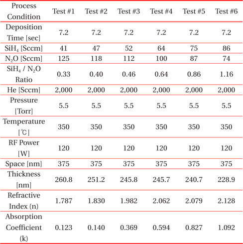
Thickness, refractive index and absorption coefficient of SiON film as a function of SiH4/N2O gas flow ratio in the deposition process
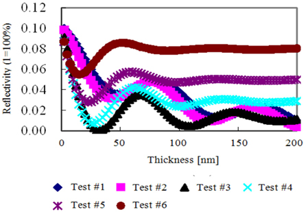
Figure 5 shows the reflectivity of BARC / PR interface for 0.13-μm-device. it was simulated with variations of the refractive indexes and the absorption coefficients in Table 2 as a function of the thickness of SiON film including the consideration of information on sub-layer. The typical sinusoidal curves were obtained with the thickness of SiON film in all conditions. The first minimum reflectivity point (λ / 4n) moved toward the thicker values with increases of the refractive index and the absorption coefficient; the first minimum reflectivity point decreased to the lowest reflectivity value of 0.04% with increases toward the refractive index and the absorption coefficient of 1.89 and 0.369 (test #3), respectively. The thickness was 33.0 nm at this condition. Then, the first minimum reflectivity point increased with increases beyond this condition. This condition (thickness of 33.0 nm, refractive index of 1.89, and absorption coefficient of 0.369) was applied to the actual substrate as the most appropriate condition which had the minimum reflectivity of BARC / PR interface for 0.13-μm-device. The pattern was formed by using PR (UV135) at the condition of test #3 including SiON as BARC layer and SiO2 of 5.0 nm as a barrier layer of SiON and PR after preparing the sub-layer for 0.13-μm-device. The increased interface roughness reduces the oscillation in the reflectivity curve rapidly [14]; therefore, the reflectivity control is difficult for the conditions of test #4, #5, and #6 due to the disappearance of oscillation at these conditions. Figure 6 shows the cross-sectional SEM images of BARC / PR interface for 0.13-μm-device demonstrated experimentally with the optimum condition (test #3) obtained by the computational simulations for optimizing thickness, refractive index and absorption coefficient of SiON film for the minimum reflectivity; this had the accurate CD control successfully without any standing wave. Deposition process of SiON as BARC for adjusting the optimum combination of thickness, refractive index and absorption coefficient with the different SiH4/N2O gas flow ratios was very effective to suppress the standing wave by absorbing light and creating destructive interference to give little reflectivity at the BARC / PR interface.
The trends of refractive index and absorption coefficient of SiON film as BARC layer were analyzed by experimental demonstration with various conditions of PR and sub-layer; the optimum condition for SiON film (thickness of 33.0 nm, refractive index of 1.89, and absorption coefficient of 0.369) was obtained by computational simulation to minimize the reflectivity of BARC / PR interface. The lowest reflectivity was 0.04% at this condition. This optimum condition for BARC SiON film was applied to the process condition for 0.13-μm-device. The optimum SiON film as BARC to PR and sub-layer could be formed with the accurate CD control and no standing wave for the nanometer-scaled semiconductor manufacturing process.