We have investigated the effects of an Ag capping layer on the emission characteristics of transparent organic light-emitting devices with Ca/Ag double-layer cathodes. The thickness of the Ag layer was varied from 10 to 30 nm, whereas the Ca was fixed to be a 10 nm in the Ca/Ag structure. The luminance and current efficiency on the cathode and anode sides are significantly dependent on the Ag thickness. For example, the current efficiency on the anode side increases from 8.4 to 11.7 cd/A, whereas, on the cathode side, it decreases from 3.2 to 0.2 cd/A as the Ag thickness increases from 10 to 30 nm. These changes in emission characteristics were investigated by measuring electroluminescence, transmission, and reflection spectra.
Organic light-emitting devices (OLEDs) consisting of functional organic thin films between the cathode and the anode have attracted much attention during the past few decades because they can provide high-performance displays and lighting applications due to their superior characteristics, such as wide viewing, fast response, and high brightness [1,2]. Because the organic layers in OLEDs are typically transparent in the visible range [3], new applications, such as see-through displays and lighting for automobile windshields, architectural and shop windows, and eyewear can be realized if both electrodes are transparent. Indium tin oxide (ITO), which is widely used as an anode material for OLEDs, has a high transparency; therefore, the use of transparent cathodes in realizing transparent OLEDs has become an area of interest. Since the first report on thermally evaporated LiF/Al/Ag semitransparent cathodes by Hung et al. [4], many researchers have focused on the evaporated semitransparent metal cathodes because they provide highly transparent and efficient OLEDs without rendering damage to the underlying organic layers. Several semitransparent metal cathodes of Sm/Au, Yb/Ag, Ca/Mg, Ca/Ag, Ba/Ag, and Sr/Ag have been proposed [5-11]. Doublelayer Ca/Ag can be an efficient cathode for transparent OLEDs because of its high transparency and low resistivity [8]. The Ca layer, which has a low work-function, makes an easy injection of electrons, whereas the Ag capping layer improves the lateral electrical conductance of the cathode [8,9].
Because the light generated inside the device is emitted out of the cathode and anode sides in transparent OLEDs, the emission characteristics, such as efficiency and electroluminescence spectrum, may be different on both sides, by the several factors, such as the microcavity effect and transmittance of electrodes. In this paper, we have investigated the emission characteristics of transparent OLEDs with semitransparent Ca/Ag cathodes on the cathode and anode sides. We have studied the effects of an Ag capping layer on the luminance, electroluminescence spectrum, and current efficiency characteristics of transparent OLEDs. We will discuss the emission characteristics of transparent OLEDs on both sides in terms of microcavity effect and optical characteristics of electrodes.
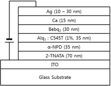
Transparent OLEDs were fabricated on ITO-coated glass substrates. The sheet resistance of the ITO film was about 10 Ω/sq. After defining ITO anode patterns using a standard photolithography process, the substrates were cleaned with isopropyl alcohol and deionized water. Then, the patterned ITO substrates were exposed to oxygen plasma. All the organic and metal layers were deposited using a vacuum thermal evaporation method in a base pressure of about 1 × 10⁻⁶ Torr. A 70 nm-thick 4,4',4"-tris[N-(2-naphthyl)-N-phenyl-amino]-triphenylamine (2-TNATA) layer was deposited on the patterned ITO substrate, and followed with the deposition of a 35 nm-thick 4,4'-bis-[N-(1-naphthyl)-N-phenyl-amino]biphenyl (α-NPD) layer. Next, a 35 nm-thick tris-(8-hydroxyquinoline) aluminum (Alq3) layer was co-deposited with 1 wt.% fluorescent dopant, 10-(2-benzothiazolyl)-1,1,7,7-tetramethyl-2,3,6,7-tetrahydro-1H,5H,11H-[1]-benzopyropyrano[6,7,8-ij]quinolizin-11-one (C545T). Then, a 30 nm-thick bis(10-hyroxybenzo[
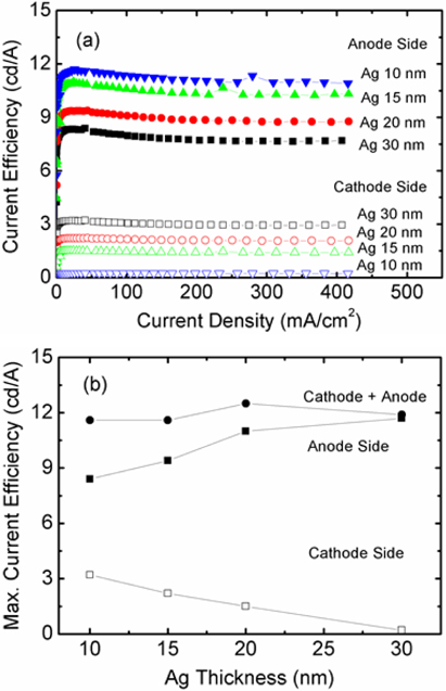
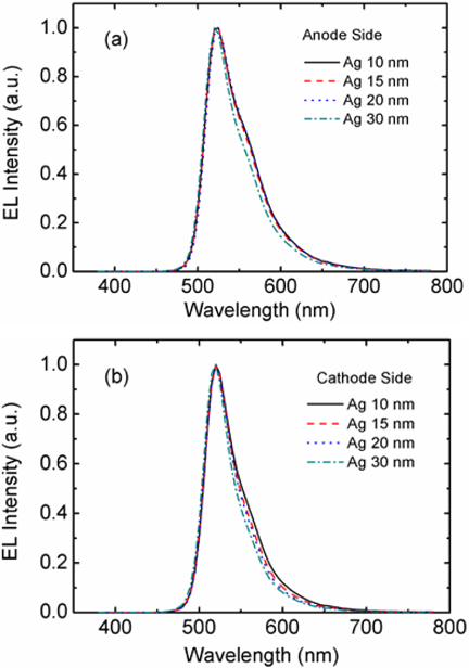
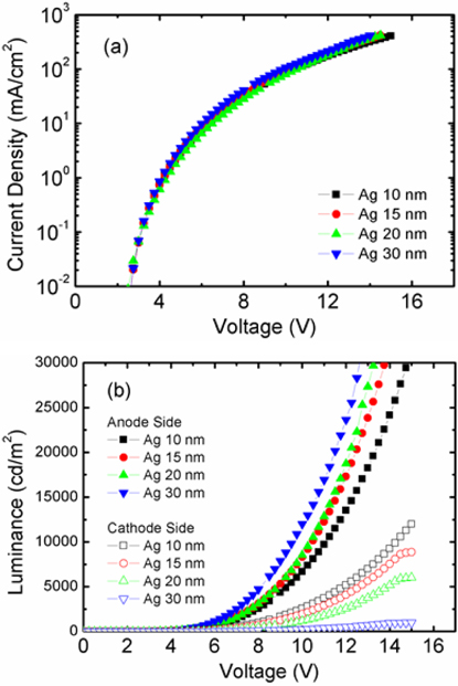
Figure 2(a) shows the current density curves as a function of voltage for the transparent devices with the Ca/Ag cathode. The thickness of the Ag layer was varied from 10 to 30 nm, whereas the Ca layer was fixed to be 15 nm. The figure shows that the current density is not seriously changed by varying the Ag thickness, indicating that the electron injection and transport are not modified by the Ag layer, since the electron transporting Bebq2 layer is not contacted with Ag, as shown in the device structure of fig. 1. The sheet resistance of the Ca/Ag cathode was about 15 ohm/sq. The Ag capping layer provides the lateral electrical conductance, while the low work-function of Ca (2.9 eV) results in easy injection of electrons from the Ca/Ag cathode into the Bebq2 layer [10]. Figure 2(b) shows the luminance curves measured on the cathode and anode sides for the devices with Ca/Ag cathodes. The luminance curves were measured on both electrode sides because the devices are semitransparent. The figure illustrates that the luminance curve is significantly modified by the Ag thickness. The luminance measured on the cathode side decreases with increasing Ag thickness at a fixed voltage. For example, the cathode-side luminance decreases from 2,560 to 240 cd/m2 at a voltage of 10 V as the Ag thickness increases from 10 to 30 nm. By contrast, the anode-side luminance increases with increasing Ag thickness. For example, as the Ag thickness increases from 10 to 30 nm, the luminance on the anode side increases from 6,690 to 11,990 cd/m2 at a voltage of 10 V. Figure 3(a) shows the current efficiency curves on the cathode and anode sides as a function of current density for the transparent devices with various thicknesses of Ag layers. Because the current density is not influenced by the Ag thickness, as shown in fig. 2(a), the current efficiency curves are consistent with the luminance curves of fig. 2(b). As the Ag thickness increases, the cathode-side current efficiency decreases but the anode-side efficiency increases at a fixed current density. In fig. 3(b), the maximum current efficiency as a function of Ag thickness for the transparent devices with Ca/Ag cathodes are clearly shown. Similar to fig. 3(a), the maximum current efficiency on the cathode side decreases from 3.2 to 0.2 cd/A, whereas, on the anode side, it increases from 8.4 to 11.7 cd/A as the Ag thickness increases from 10 to 30 nm. The figure also shows that the sum of the maximum current efficiencies on both the cathode and the anode side is almost same as the Ag thickness. These results suggest that the Ag thickness influences the extraction of light out of the cathode and anode, rather than the number of photons generated inside the device. The extraction efficiency on both of the electrode sides may be altered by the microcavity effects, because the reflective Ag layer may cause multiple interferences [12]. Figure 4 shows the electroluminescence spectra measured on the cathode and anode sides for the transparent devices with various Ag thicknesses. The emission spectrum on both electrodes is not changed significantly but it is narrowed slightly by increasing Ag thickness, thus indicating the weak microcavity effects [13]. The finding suggests that the changes in the extraction of light on both electrodes by varying the Ag thickness may be caused by the transmittance and reflectance of the cathode rather than the multiple interference effects between both electrodes.
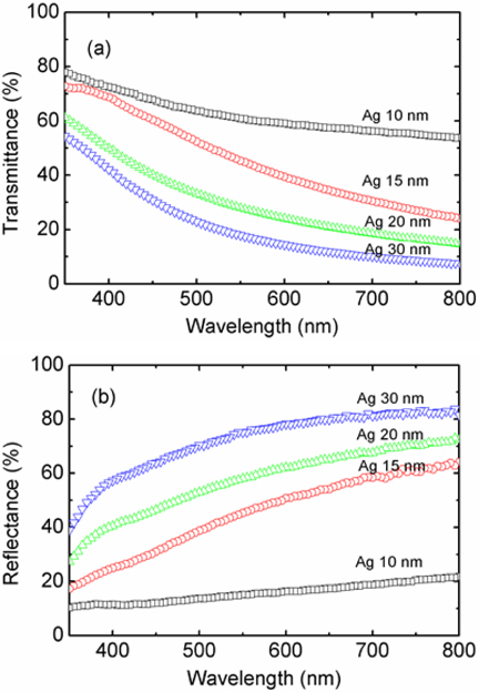
Figure 5 shows the transmission and reflection spectra for the Ca/Ag cathode with different thicknesses of Ag layers coated on the glass substrates. As the Ag-layer thickness increases, the transmittance of the Ca/Ag cathode decreases, whereas the reflectance increases. For example, fig. 5(a) shows that the transmittance of the Ca/Ag decreases from 62% to 21% at the wavelength of 520 nm, which is the emission wavelength of the fluorescent dopant, C545T molecule, as the Ag thickness increases from 10 to 30 nm. That finding indicates that the extraction of light out of the Ca/Ag cathode decreases with the increasing Ag thickness, which results in the decrease of luminance and current efficiency on the cathode side. However, fig. 5(b) shows that the reflectance increases from 24% to 72% at the 520 nm as the Ag thickness increases from 10 to 30 nm. Thus, the reflection of light by the Ca/Ag cathode increases by increasing the Ag thickness. The reflected light is moving toward the ITO anode, and extracted out of the anode because the ITO electrode has a sufficiently high transmittance of 90% and low reflectance of about 1% in our devices, such that the luminance and current efficiency on the anode side increases as the Ag thickness is increased. It also should be noted that the luminance and current efficiencies on the cathode side are lower than those on the anode side in the t Ag-layer thickness range of 10~30 nm,, as shown in the fig. 2 and 3, since the transmittances (20~60%) of the Ca/Ag cathode with the Ag layer of 10~30 nm are lower than that (90%) of the ITO anode in our devices.
We have investigated the effects of an Ag capping layer on the emission characteristics of transparent OLEDs with Ca/Ag cathodes. The extraction of light generated inside the emission layer out of the cathode and anode is determined by the transmission and reflection of the Ag layer. As the thickness of the Ag layer increases, the current efficiency measured on the cathode side decreases because the transmission of light through the cathode decreases while the reflection of light increases by the reflective Ag layer. In contrast, the anode-side efficiency increases with increasing Ag-layer thickness, as the reflected light by the Ag layer is extracted out of the anode.