This paper presents the structure and process technology of simple and low-cost wafer-level packaging (WLP) for thin film radio frequency (RF) devices. Low-cost practical micromachining processes were proposed as an alternative to high-cost processes, such as silicon deep reactive ion etching (DRIE) or electro-plating, in order to reduce the fabrication cost. Gold (Au)/Tin (Sn) alloy was utilized as the solder material for bonding and hermetic sealing. The small size fabricated WLP of 1.04×1.04×0.4 mm3 had an average shear strength of 10.425 kg/mm2, and the leakage rate of all chips was lower than 1.2×10⁻⁵ atm.cc/sec. These results met Military Standards 883F (MIL-STD-883F). As the newly proposed WLP structure is simple, and its process technology is inexpensive, the fabricated WLP is a good candidate for thin film type RF devices.
Recently, as electronic components for portable wireless devices grow ever lighter, thinner, and smaller, their everincreasing complexity and miniaturization is also required [1- 3]. Among them, RF components like the film bulk acoustic resonator (FBAR) filter, transform high-frequency electrical signals into low-frequency acoustic signals, and then after filtering, transform the signals back into high-frequency electrical signals. Miniature RF passive devices fabricated in the form of thin films on silicon substrates have the advantage of enabling ultra-thin packaging. Practical packaging methods have undergone a series of processes, such as cutting wafers into individual chips, cleaning chips, chip bonding to the lead frame or ceramic substrate, wire bonding, and molding with a metal case or epoxy. These processes not only require a lot of effort, but also do not offer a high yield. Currently, as an improvement on the practical method, WLP has emerged as the packaging method for thin film type RF devices. The devices are capped with a processed silicon or glass wafer at wafer level. After the packaging process is completed, chips are separated from the wafer [4]. Therefore, WLP has many advantages of simplification of the package, miniaturization of component, and cost reduction.
At present, the thickness of RF components demanded for portable wireless devices is less than 0.4 mm. If it is assumed that a device wafer and a package wafer have the same thickness, the thickness of the package wafer should be about 0.2 mm. Such a thin wafer is difficult to handle in the manufacturing process. In addition, a package wafer in the WLP should simultaneously conduct the functions of protecting of the devices from the external environment, and of connection of the input and output terminals to the outside. The characteristics of a RF device may change, due to the attachment of dirt, moisture, and even light atoms, like oxygen and carbon [5-7]. Electrical through-interconnection and hermetic sealing are necessary, in order to connect the input and output terminals, and protect the device from the external environment [8-10]. Most of the WLP makers, such as STMicroelectroincs, VTI Technologies, and Silex Microsystem, fabricate the package wafer using silicon DRIE, and the hole-filling method with metal. However these processes result in higher cost, and lower throughput [11-13].
This paper proposes a simple, low-cost, three-dimensional silicon process technology to design and fabricate a small and thin WLP for thin film type RF devices. In order to fabricate a package wafer, expensive processes such as silicon DRIE and plating method were avoided, and low-cost practical micromachining technology was used instead, including silicon anisotropic wet etching, and metal deposition methods. A dummy wafer with a micro strip line was used to evaluate the seal characteristics of the package, instead of the actual thin film type RF device. In addition, the package wafer and the dummy wafer were bonded with Au/Sn alloy, to complete the WLP. The finished WLP was separated into individual chips, and then their shear strength and leak rates were evaluated.
2. DESIGN AND FABRICATION OF THE WLP
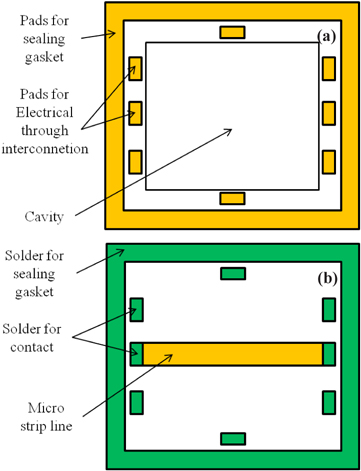
For fabrication of a practical WLP, holes were formed in a package wafer using the silicon DRIE method, and filled with copper or poly silicon. Unlike that method, the proposed WLP was fabricated using silicon anisotropy wet etching, a sloping plane photographic process, and metal deposition. The schematics of the package and dummy wafer for the proposed WLP are illustrated in Fig. 1. A package wafer consists of cavities for the devices, electrical through-connection, a wire-bonding pad for connecting to the outside circuit, and a sealing gasket for hermetic sealing, as shown in Fig. 1(a). Au/Sn solder was used to bond the wafers. The Au/Sn solder has very excellent properties as a wafer bonding material, in that it has very low leakage rate, high electrical conductivity, and high bond strength. Another advantage of Au/Sn solder is that it can concurrently provide wafer bonding, hermetic sealing, and electrical connection between the dummy wafer and the package wafer.
Anisotropic wet etching was used to form through-holes. Anisotropic wet etching has the etching shape of a reverse pyramid, and the etching depth can be precisely controlled. Its disadvantage is that because the surface area is very large, compared to the bottom area of via holes, a large number of via holes may not be formed on a limited area. Fortunately, it is not a problem in the case of most thin film type RF devices, including FBAR, because they do not have a large number of input and output terminals. The location of the electrical through-connection is right above the input and output terminals from the bottom of the cavity, which reduces parasitic inductance, by shortening the length of interconnection.
A micro strip line was formed on the dummy wafer, instead of the actual thin film type RF devices wafer, and metal and solder patterns were simultaneously deposited on the dummy wafer, as shown in Fig. 1(b). In developing a package, it is most ideal to utilize an actual RF device wafer. However, much cost and time are required to fabricate a device wafer, and there are some technical difficulties, in that the mask design drawing should be shared with the device manufacturing company. Therefore, a dummy wafer with micro strip line was designed and fabricated to replace the device wafer. Although it is a dummy wafer, the size, location, and number of electrodes were determined as for the actual device. The size of one package was 1.04×1.04×0.4 mm3, which was the same as the chip size. The cavity in each individual package was designed to be a square, of side length 520 μm. The width of the gasket for bonding and sealing of the wafer was set at 80 μm. Here, the junction area of the sealing gasket became 0.303 mm2. The size of contact pad connected with the input and output terminals of a dummy wafer was designed to be 35 μm × 110 μm, in consideration of the mechanical junction strength and electrical contact resistance, and eight pads were assigned to one chip. Therefore, the total pad area became 0.012 mm2. The micro strip line was 860 μm in length, and 160 μm in width. The width and length of the solder pattern situated on the metal pad, were smaller by 5 μm, than those of the metal pad. Here, except for two pads needed for the micro strip line, the remainder of the pads have the function of merely connecting the upper and lower parts of the package wafer. The entire bonding area, i.e. the sum of the border junction area at the border of the package and the contact pad area, was designed to be 0.315 mm2. The wire bonding pads were formed on the upper side of the package wafer, to make connection with the outside circuit.
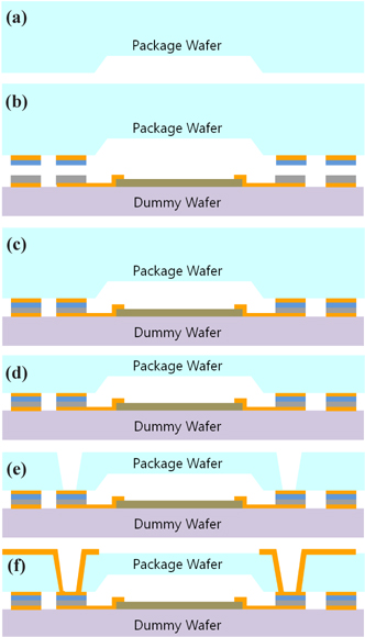
Figure 2 shows the fabrication processes of the WLP. A 4 inch (100) silicon wafer with resistivity of higher than 10 kΩ·cm was used, in consideration of the RF characteristics [14]. Its thickness was 300 μm. First, silicon nitride (Si3N4) thin film with a thickness of 50 nm was deposited on both sides of the package wafer, using a low pressure chemical vapor deposition (LPCVD) method. The etching window for silicon anisotropic etching was made, by a reactive ion etching (RIE) method. Then, a 20 μm-depth cavity was formed, by etching silicon in tetramethyl ammonium hydroxide (TMAH) solution (Fig. 2(a)). Next, Si3N4 was stripped with 49% hydrofluoric acid solution, and the lift-off pattern for the metal line was formed with negative photoresist. Because the metal patterns were made around the 20 μm-depth cavity, a spray coating method was utilized, with better step coverage than the spin coating method. Then, an electron beam evaporator was used to deposit a multi-layer metal pattern. The metal pattern concurrently performed the functions of electrical interconnection, and under-bump-metallization (UBM) for solder bonding. Only low electrical resistance was required for the interconnection; however, different requirements should be met for the UBM. Usually, the UBM has three layers: a lower layer with good adhesion to sil-icon, a middle layer with good wettability to solder materials, and an upper layer with antioxidant function. In this paper, the Cr/ Ni/Au structure was used for the UBM of Au/Sn solder. The thickness of each layer was 100 nm, 200 nm, and 500 nm, respectively. For solder, Au with the thick of 4 μm was deposited on the UBM of the package wafer (Fig. 2(b)). Metal pads with micro strip line patterns were formed in the same way as the UBM of the package wafer. Sn with the thickness of 2.9 μm was deposited on the UBM of the dummy wafer, using an electron beam deposition method. Au with the thickness of 0.08 μm was deposited on the surface of Sn, to prevent its oxidation (Fig. 2(b)).
The fabricated package and dummy wafers were bonded for 20 minutes at a temperature of 285℃, and a pressure of 5,000 N (Fig. 2(c)). Then the backside of the package wafer was ground to a thickness of about 100 μm, so that the chip had a total thickness of 400 μm (Fig. 2(d)). After finishing the grinding process, organic and non-organic contaminants that resulted from the grinding process were removed by a cleaning process; and then an etching mask for via hole etching was formed. Since a via hole is formed using the anisotropic wet etching process of silicon, silicon nitride or silicon dioxide thin films is appropriate as an etching mask. Because a bonded wafer has solder materials with a low melting point, the process for an etching mask required a temperature that was as low as possible. In this paper, 300 nm thick SiNx thin films were formed at 250℃, using a plasma-enhanced chemical vapor deposition (PECVD) method. Because the entire bonded wafer enters into the etching solution for etching, SiNx, the same as on the front side, was deposited on the backside of the bonded wafer in order to protect it. Then, via holes were formed, by etching the silicon in the TMAH solution (Fig. 2(e)). Lastly, metal patterns for electrical through-connection and wire bonding pads were formed. In the same way as described earlier, the metal pattern was formed by photography, metal deposition, and the lift-off. The structure of the metal layer was Ti (100 nm)/Ni (200 nm)/ Au (1,000 nm) (Fig. 2(f )).
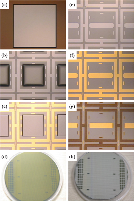
Figures 3(a) to (d) show the result of each process for the package wafer. Figure 3(a) is an image of the trench with the depth of 20 μm at the center of an individual package. Figure 3(b) shows the lift-off photoresist pattern to form the UBM, using a spray coating method. Figure 3(c) shows the precise formation of the metal line around the trench. Figure 3(d) shows the completed package wafer. Figures 3(e) to (h) show the result of each process for the dummy wafer. Figures 3(e) and (f) are images of the photoresist pattern for a micro strip line, and the UBM on the dummy wafer, respectively. Figure 3(g) shows the formation of Au/ Sn solder, and Figure 3(h) is the image of the completed dummy wafer.
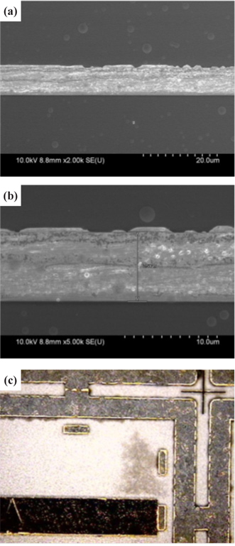
The fabricated package and dummy wafers were bonded, and Fig. 4 displays the scanning electron microscopy (SEM) images. As shown in Figs. 4(a) and (b), the bonding interface between the dummy wafer and the package wafer is obviously still divided; but large voids or cracks are not observed on the interface [15]. Figure 4(c) shows a photo of the bonding surface, after forcibly taking off the bonded wafer. The solder has uniformly melted on the metal pad.
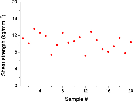
After dicing the bonded wafer, 20 chips were randomly selected to measure the bonding strength. According to the Military Standard 883 F (MIL-STD-883F), a package of smaller than 5×10⁻⁴ inch2 (0.32 mm2) should be able to endure shear stress of larger than 0.04 kg/10-4 inch2 (0.062 kg/mm2) [14]. As shown in Fig. 5, the average shear strength and standard deviation of the fabricated chips were 10.425 kg/mm2 and 1.89 kg/mm2, respectively. The whole bonded area of the proposed package is 0.315 mm2; and therefore, the chips have excellent bonding strength that exceeds the standard. However, the difference of shear strength among chips was believed to be caused by the factor that the package wafer was slightly bent overall under the bonding process, because there was the difference in the thermal expansion coefficients of silicon and the solder materials, of gold, nickel, and titanium. These results significantly affect the yield of the products.
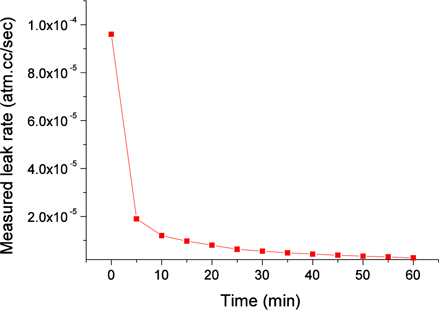
In order to evaluate the sealing characteristics of the bonded chips, helium (He) bombing and leakage characteristics were tested. The He leakage tests were not measured from a single chip but four-pieces divided from the wafer were measured. Four pieces divided from the wafer were placed in the pressure chamber. The pressure in the chamber was raised to 5 atmospheres by using flowing He gas, and this state was maintained for 6 hours. Next, the pieces were transferred to the leak test chamber, and a mass spectrometer was used to measure the leak rate. The He leakage from the samples was measured every five minutes. Figure 6 shows the result of leakage characteristics measured at an interval of five minutes, for up to sixty minutes. The early leakage rate was about 10-4 atm.cc/sec, and reached a stable state in about 10 minutes, to be lower than 1.2×10⁻⁵ atm.cc/sec. Because the initial amount of He was extracted from the surface of the package, the leak rate was high; however, it dramatically reduced over time. These results showed that the fabricated WLP sealed hermetically. Given that more than 5,000 chips are included in one wafer, the leakage rate per chip is approximately lower than 1×10⁻⁸ atm.cc/sec. This meets the Military Standard 883 F (MILSTD- 883F) that prescribes the leakage rate should be lower than 4.94×10⁻⁸ atm.cc/sec [14].
In this paper, a simple, low-cost WLP was designed and fabricated for thin film type RF devices. Electrical through-connection was formed, using practical silicon anisotropic etching and a metal deposition method. The package wafer included cavities for devices, electrical feed-throughs for electrical connection, and a solder for the bonding of a device wafer. The size of the fabricated WLP chips was 1.04×1.04×0.4 mm3, and they exhibited excellent mechanical properties. The average shear strength was 10.425 kg/mm2, and the leakage rate of all chips was 1.2×10⁻⁵ atm.cc/sec. The proposed WLP has a simple structure, and uses a low-cost process; therefore, it is appropriate as a package for thin film type RF devices. In our next paper, the research result on the electrical characteristics and yield improvement of the proposed WLP will be introduced.