A charge pump is used to generate a voltage that is higher than that of the power supply, without an amplifier or transformer. Many charge pump circuits are based on the Dickson charge pump [1,2] which provides high voltages by transferring the charge into a load capacitor. The Dickson charge pump is a voltage multiplier circuit similar to the classic Cockcroft-Walton multiplier. A charge pump circuit can be used as the capacitorswitched DC-DC boost converter which operates by switching the connection mode of a few boosting capacitors with the load capacitor.
In the Dickson charge pump circuit, two phase clocks are out of phase with each other and successively charge during each half of the clock cycle. However, as the number of pumping stages is increased, the output voltage is decreased due to the body effect of the diode-connected MOS transistor. As the threshold voltage of the diode-connected MOS transistor increases due to the body effect, the voltage gain per unit stage decreases and the output voltage is lower than the expected value. The pumping efficiency decreases as the number of stages increases. Another disadvantage of the application of the regulator is the large ripple voltage. In the switching-mode converter with the LC filter [3-5], the ripple voltage can be reduced by varying the passive parameters. However, in the case of a conventional regulated charge pump, the regulator pumps the capacitors with full power and causes a large ripple voltage which is independent of the load resistance. To reduce the ripple voltage, the feedback control circuit is proposed in the charge pump circuit. Another advantage of the introduction of the feedback circuit is that it can generate constant output voltages regardless of the load current. The function of the feedback circuit is to make the output proportional to the input and to reduce the contribution to the output noise due to the circuit components.
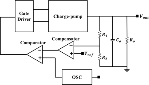
The proposed converter shown in Fig. 1 is composed of a switching charge pump stage and feedback control circuit. Among the various elements in the control circuit, the error amplifier and the output buffer in the control circuit are important for the performance of the overall feedback control which requires fast dynamic response and a correct duty signal. The error amplifier in the control circuit requires a high gain in the differential pair and high current-driving capability in the current sources to obtain a fast transient response without the slewing problem. The input of the compensator includes the output volt age which is scaled down by the R1 and R2 resistances.
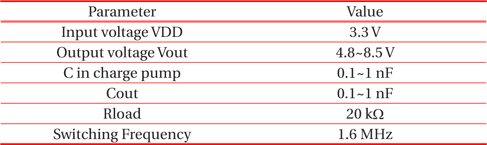
In order to provide low power and a fully integrated power module for the boost converter in the display driver circuit, a capacitor-switched charge pump with a feedback control circuit is designed with a standard 0.35 μm CMOS process.
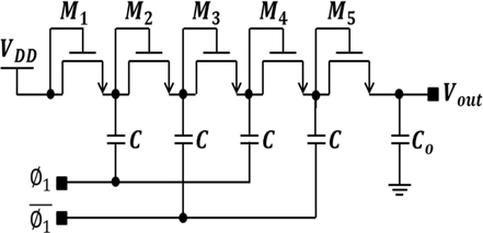
In the Dickson charge pump circuit as shown in Fig. 2, voltages higher than the input voltage are obtained by the charge pumping. The diode-connected MOSFETs in the charge pump cause a shift in the threshold voltage due to the body effect. The output voltage cannot be a linear function of the number of stages and its efficiency decreases as the number of stages increases. In this work, a four-stage charge pump circuit with feedback control is used for the boost converter to reduce the ripple and obtain an output voltage independent of load resistance. The fourstage charge pump circuit has 5 MOS switches and 4 capacitors. By employing the feedback circuit, the output voltage can be constant and stable with a variation of the source input or load resistance. Although the body effect and the threshold shift cannot be omitted because of the operation of the charge pump, the required output voltage with a small ripple can be obtained by the feedback circuit.
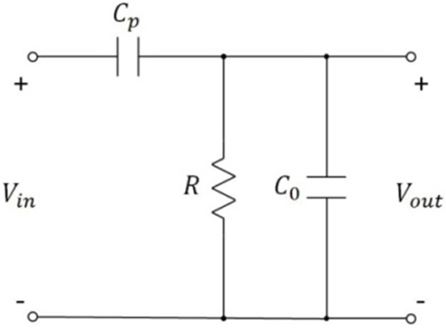
Figure 3 shows a modified circuit diagram of the charge pump circuit which includes the output resistance Ro and capacitance Co. The pumping capacitance Cp is assumed in the series connection of the capacitance C, which is controlled by the clock pulse. The pumping capacitance Cp also depends on the number of stages. Therefore, the pumping capacitance Cp is the capacitance divided by the number of stages.
Based on the charging or discharging operation of the charge pump, the transfer function for the frequency response can be written as an approximation
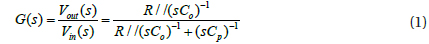

where R, Co, and Cp are the resistance, output capacitance, and pump capacitance, respectively. The frequency response and stability are determined directly by their pole or zero. We can determine whether or not the converter circuit is stable by examining the loop gain as a function of frequency.
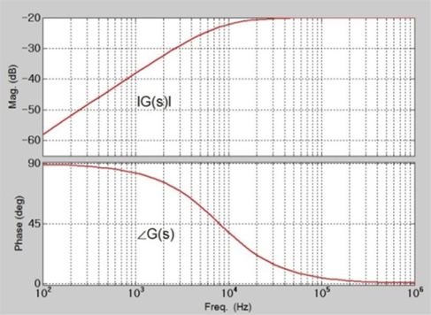
The frequency response of the transfer function is shown in Fig. 4, which is drawn in the Bode plot. In terms of the phase margin for the stability concern, the plot indicates a stable frequency response which has a sufficient positive phase margin in the measured frequency range. The frequency response is stable because of the single pole and zero in the transfer function of equation (2). Table 1 summarizes the circuit parameters of the charge pump circuit.
[Table 1.] Circuit parameters of the charge-pump.
Circuit parameters of the charge-pump.
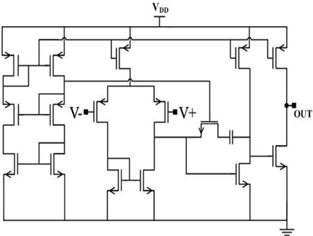
The feedback control circuit is a CMOS integrated circuit (IC) for chip minimization. The operational amplifier (op-amp) shown in Fig. 5 is used as an error amplifier which is composed of current mirrors, an input differential stage, and a source follower. The compensating circuit can be added for the stability of frequency response and a fast response-time. The conventional compensator is usually composed with an operational amplifier, resistors, and capacitors to generate poles or zeros. In this operational amplifier, a high-gain differential stage is used for the high speed operation of the control circuit. A cascode circuit is used for the current source in the differential stage.
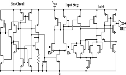
Figure 6 shows the comparator in the control circuit which provides duty signals to the charge pump. The comparator is composed of a bias circuit, an input differential stage, and a latch. The bias circuit in front of the differential stage is used for the current source to proceed to the input differential stage. The input differential stage is an active-loaded amplifier. The latch is used for a clear logic response.
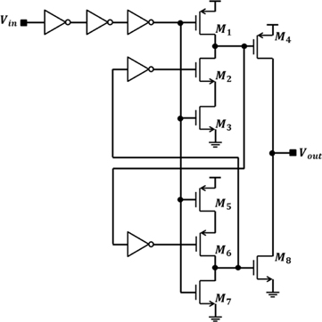
The buffer and oscillator are shown in Fig. 7 and Fig. 8, respectively. The gate driver is composed of the two buffers which operate inversely to each other. The buffer in Fig. 7 is composed of CMOS inverter chains, power transistors, and a feedback loop. CMOS inverter chains have different aspect ratios which depend on the channel length and width. A conventional buffer is usually composed of CMOS inverter chains without feedback. It consumes the short-circuit power because of the simultaneous turn-on of the up/down transistors in the inverter. A feedback controlled CMOS buffer [7] is shown in Fig. 7. It eliminates the short-circuit power consumption. The feedback signal from the M4 and M8 transistors is used to control the gate driving signal so that the M4 and M8 transistors do not switch simultaneously. No time delay occurs when the transistors are turned on simultaneously. Therefore, the short circuit can be eliminated with a reduction of the propagation delay.
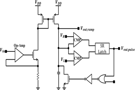
The sawtooth wave generator shown in Fig. 8 is used to obtain a ramp signal for the input of the comparator. It is implemented by a NOR gate as the feedback. The peak voltages of the ramp signal are obtained from the VH and VL inputs shown in Fig. 8.
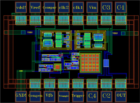
The circuit in Fig. 1 is designed in 0.35 μm CMOS technology with 2-poly and 4-metal process. The layout photo is shown in Fig. 9. The contact holes and metal interconnection are symmetrically laid out around the circuit to minimize signal noise. The circuit has an area of 1 mm2.
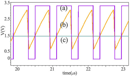
Figure 10 shows the output wave forms of the comparator (a), ramp signal (b), and error amplifier (c). The figure is taken from the Cadence layout simulation shown in Fig.1, which includes the charge pump and control circuits. By comparing the ramp signal with the amplifier output, the duty signal of 66% is obtained as expected.
In the switching converter with the LC filter, the ripple usually results from the on-off switching devices in the power block, which causes a relatively large ripple ratio. The ripple results from the charging and discharging charges across the inductance. On the other hand, in the charge pump regulator, the ripple occurs from the pumping and blocking periods across the charge pump. The pumping current into the capacitor determines the ripple voltage, which is also inversely proportional to the switching frequency.
The output voltage of the charge pump regulator with n stages can be approximated by the following [8,9];
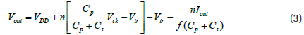
where VDD, Vck, Cp, Cs, f, and Iout are the input voltage, clock voltage, pump capacitance, stray capacitance, frequency, and output current, respectively. Vtr is the voltage associated with the switching- on resistance in the MOSFET. The output voltage is reduced by the ratio of the pump and stray capacitances. The output voltage increases with an increase of the number of pump stages, but it is not a linear function of the number of stages.
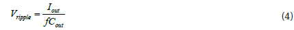
The ripple voltage is defined as the following, if stray capacitance is ignored [10].

where Cout, f, and Iout are the output capacitance, frequency, and output current, respectively. The ripple voltage depends on the output capacitance and the switching frequency.
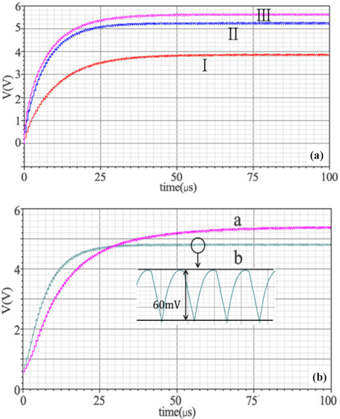
The pump current is proportional to the output current Io. The output voltages of the charge pump regulator shown in Fig. 11 are obtained with the variation of pump capacitance or output capacitance Co. In Fig. 11(a), the pump capacitance is increased from 0.1 nF to 1 nF with the constant output capacitance of 1 nF. This shows that the output voltage increases with an increase of the pump capacitance, which is from 3.8 V to 5.6 V. On the other hand, when the output capacitance increases at the constant pump capacitance, the output voltage is almost constant as shown in Fig. 11(b), although the settling time is longer with higher output capacitance. The result means that the output of the charge pump depends more on the pump capacitance and corresponds to the equation (3).
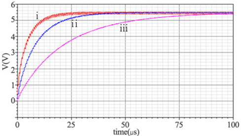
The output voltage of the charge pump regulator, which has the feedback control circuit, is studied with the variation of the number of pump stages. Figure 12 shows the output voltages at the 4 stages (a) and 8 stages (b) regulator, which has the same feedback circuit. The output voltage increases from 4.8 V to 5.3 V with higher pump stages. The ripple voltage is obtained as 60 mV and is independent of the number of pump stages. On the other hand, without the feedback control circuit, the ripple voltage is obtained as over 100 mV and increases with higher pump stages. The advantage of the application of the feedback control circuit is shown in this result, which means that the ripple voltage is significantly reduced and is almost independent of the number of stages. The proposed converter achieves a high figure of merit with a small output current of 0.24 mA and ripple voltage of 60 mV.
The advantage of the low output current and ripple can be applied for the LED display driver circuit which usually uses a current of under 10 mA. The performance of the designed 4-stages charge pump regulator that has the feedback control circuit is shown in Table 2.
[Table 2.] Performance of the proposed charge-pump.
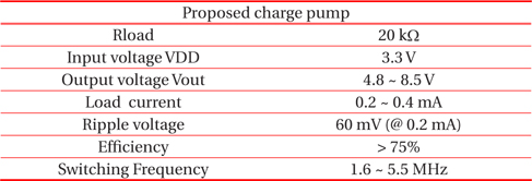
Performance of the proposed charge-pump.
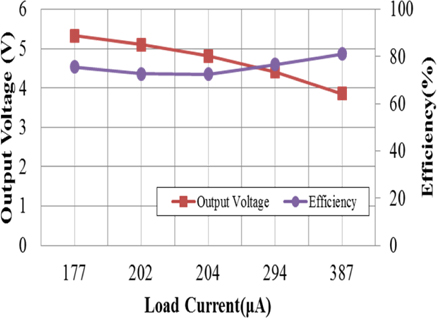
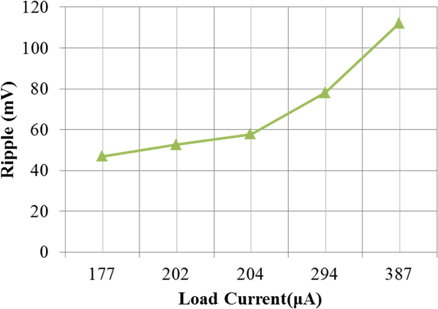
Figure 13 shows the output voltage and efficiency with variation of the load current. As the load current increases, the power efficiency is almost constant at 75% and the output voltage decreases. This indicates that the efficiency is almost independent of the load current in the measured current range. However, when the load resistor becomes smaller with high frequency, the dynamic power loss is relatively larger than the static power loss and the efficiency can be reduced because of the switching noise. The ripple voltage with variation of the load current is shown in Fig. 14. The result corresponds to the dependency which can be obtained from the equation (4) and the ripple voltage is proportional to the load current. The ripple voltage is under 60 mV at the load current of 0.2 mA.
This paper describes a charge pump boost converter with an integrated CMOS control circuit. The feedback control circuit is applied in order to obtain a small ripple voltage that is almost independent of the load resistance. The feedback circuit operates with an error amplifier, a comparator, and an oscillator. The simulation test shows that the 0.35 μm CMOS boost converter with 2-poly 4-metal operates at an output voltage of 4.8 ~ 8.5 V, with an input voltage of 3.3 V and frequency of 5.5 MHz. The proposed charge pump regulator achieves a high figure of merit with a small output current of 0.4 mA with a high power efficiency of 75%, which is applicable for high performance LED display driver circuits.