Emission properties of the organic light-emitting diodes were investigated with the use of a hole-injection layer of copper(II)-phthalocyanine (CuPc). The manufactured device structure is indium-tin-oxide (ITO) (180 nm)/CuPc (0~50 nm)/ N,N'-Bis(3-methylphenyl)-N,N'-diphenylbenzidine (TPD) (40 nm)/ tris-(8-hydroxyquinoline) aluminum (III) (Alq3) (60 nm)/Al(100 nm). We investigated the luminescence properties of Alq3 which is affected by the CuPc hole-injection layer. Also, we studied the influence of light-emission properties in the structure of an ITO/CuPc/TPD/Alq3/Al device depending on the several thicknesses of CuPc (0~50 nm) layer. As a result, it was found that the hole injection occurs smoothly in the device with 20 nm thick CuPc layer, and the properties become significantly worse in the device with a CuPc layer thickness higher than 40 nm. We studied the topography and external quantum efficiency depending on the layer thickness of CuPc. Also, we analyzed the electroluminescent characteristics in the low and high-voltage range.
The organic light-emitting diode (OLED) was developed by Tang and VanSlyke of Kodak in 1987. It is a self-emissive device, and it has the advantages of a wide gamut of colors and a fast response speed. For this reason, OLED has potential possibilities for future application in flexible displays [1]. The OLED is currently being developed for many display applications. However, in recent years, the OLED has also been actively developed for the use as backlight units (BLUs) of liquid-crystal display lighting. Recently, active research has been conducted in this regard by Samsung, LG, and others, and there is a growing market for OLED BLUs. The materials used for the hole-injection layer are required to possess enhanced interfacial properties relative to the proper surface energy of the hole-injection layer because the interfacial properties are not good.
Physical properties depend on the heterojunction interface between the organic and inorganic materials for the hole-transport layer (HTL) and indium-tin-oxide (ITO) in the OLED device.
Additionally, an energy barrier at the interface is attributed to the highest occupied molecular orbital (HOMO) level of the hole-transport layer, and the work function of ITO; the HOMO level is appropriate, when it lies between the HOMO level of hole-transport layer, and the work function of ITO. To increase the external quantum efficiency, less absorption is needed in the visible light region [2]. The hole-injection materials that are typically used are copper(II)-pthalocyanine (CuPc), and poly(3,4-ethylenedioxythiophene) poly(styreneesulfonate) (PEDOT:PSS). However, PEDOT:PSS requires a spin coating process, because of the polymeric material. Thermal evaporation is not appropriate.
The CuPc has many advantageous characteristics, such as excellent thermal stability, and suitable thermal oxidation properties, compared to other organics. Its ionization energy is similar to that of ITO, and its interfacial adhesion to ITO is excellent. In addition, it allows hole injection even at low voltage, because the HOMO level of CuPc is slightly higher than the work function of the ITO electrode [2]. Additionally, a CuPc buffer layer under an Alq3 film in an OLED is reported to be useful, in improving the electrical stability of the OLED [3]. The CuPc layer prevents deterioration of not only the organic material, but also the electrode layer [4].
In the present study, in order to understand hole-transport, experiments were performed using a device with the holeinjection layer and the hole-transport layer. We also studied the characteristics of the devices with regard to the thickness of the hole-injection layer through a comparison between the devices with and without, a hole-injection layer.
In this experiment, the OLED was made using a thermal evaporating system, to make a 5 mm wide ITO anode by patterning the wet etching, and organic material was deposited using an organic mask. The anode layer was made to intersect the 3 mm wide Al cathode layer, by using a cathode mask. The total emission area was 15 mm2.
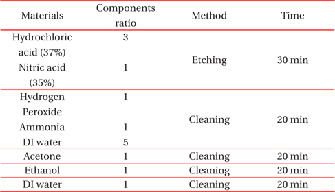
The ITO glass, having a sheet resistance of 8 Ω/□ and thickness of 180 nm, was received from Samsung Corning Co., and confirmed by four-probe meter. The 5-mm-wide ITO strip was formed by exposing the glass to a 3:1 solution of hydrochloric acid (HCl) and nitric acid (HNO3) for about 20 min at room temperature. The same reagent used in the manufacturing process for the formation of the ITO anode was used for the experiment, and is summarized in Table 1.
[Table 1.] Composition ratio of reagents used in wet etching.

Composition ratio of reagents used in wet etching.
N,N'-Bis(3-methylphenyl)-N,N'-diphenyl-benzidine (TPD), used as a hole-transport layer, was deposited to a 40 nm layer, by thermal evaporation on CuPc, purchased from Sigma Aldrich Co.Deposition of all the organic materials was performed with a slow evaporation rate of 0.5~0.3 Å/s, and it was evaporated at a base pressure of 8×10⁻⁶ Torr. The Al cathode was deposited at a rate of 4~5 Å/s. The voltage was varied from 0 V to 15 V, using LabVIEW on a programmable computer, with a Keithley 2410 1,100 V source meter. Additionally, the luminance-voltage characteristics of the OLEDs were measured, using a MINOLTA CHROMA METER CS-100A. The device is located at 15 cm distance from a light source in a dark room. A reference device was made with the structure of ITO (180 nm)/TPD (40 nm)/Alq3 (60 nm)/Al (100 nm), and the device with CuPc hole-injection layer was made with a structure of ITO (180 nm)/CuPc (x nm)/TPD (40 nm)/Alq3 (60 nm)/Al (100 nm). The measured CuPc thickness was varied, in the range of 10~50 nm.
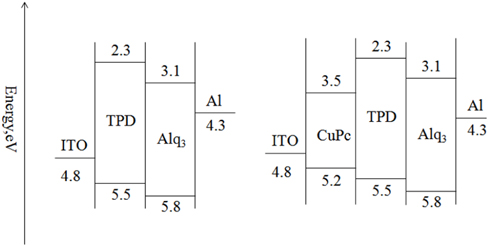
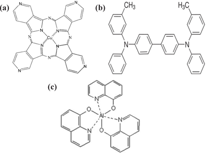
Figure 1 shows the molecular structures of CuPc, TPD, and Alq3 used in this study. The CuPc layer reconciles the inorganic of anode (ITO), and the TPD organic layer [4].
Figure 2 shows an energy-level diagram of the devices with, and without, the CuPc hole-injection layer. In the device without a hole injection-layer (0 nm), there is an energy barrier of 0.7 eV for the TPD hole-transport layer, as shown in Fig. 2(a). However, in the device with a CuPc hole-injection layer, there is an energy barrier of only 0.4 eV between the anode and the hole-injection layer, as shown in Fig. 2(b). This difference viewed from the hole side means that the device is able to emit a light with less energy supply, because of the reduced carrier-injection energy required from the anode to the emissive layer.
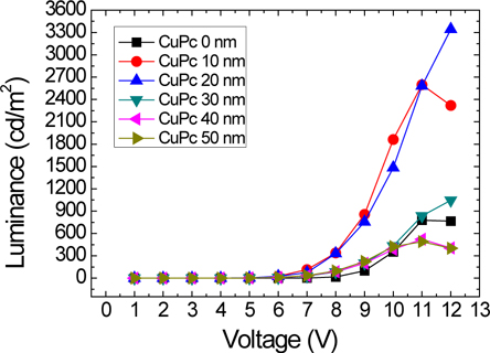
Figure 3 shows the luminance-voltage characteristics of the ITO/CuPc/TPD/Alq3/Al for several thicknesses of CuPc layer. The device without CuPc layer has a turn-on voltage of about 7 V. The maximum luminance is about 800 cd/m2, at around 12 V. The device with 10 nm thick CuPc layer exhibits better characteristics in the low voltage range of 1~9 V, and the device with 20 nm thick CuPc layer exhibits better characteristics in the high voltage range above 10 V. Experimental results show that the device with a CuPc layer of 10, 20, or 30 nm produces more luminance at the same voltage, than that of the device without the CuPc holeinjection layer. However, the devices with 40 or 50 nm thick CuPc layer show less luminance at the same voltage than that of the device without CuPc layer.
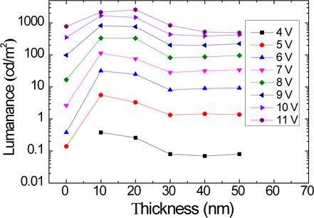
Figure 4 shows the semilog plot of luminance as a function of CuPc layer thickness in the ITO/CuPc/TPD/Alq3/Al device. The turn-on voltage of the device with CuPc layer is lower than that of the device without CuPc layer.
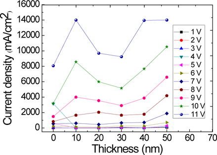
Figure 5 shows a graph of the thickness-dependent current density for the ITO/CuPc/TPD/Alq3/Al devices at several voltages. All the CuPc-deposited devices have a higher current density at the same voltage than that of the device without CuPc layer. The current density reaches its maximum value at about 11 V. At that point, the resistance is higher than that the organic layer can withstand. Thereafter, the organic material begins to undergo thermal oxidation, and the luminance decreases (See Fig. 3).
For the devices with 40 and 50 nm thick CuPc layers, more charge carriers are injected into the device with CuPc, compared with the no-CuPc device. Moreover, as the current density increases, more resistance heating occurs, and the organic layer is weakened. This was confirmed by repeating the measurements.
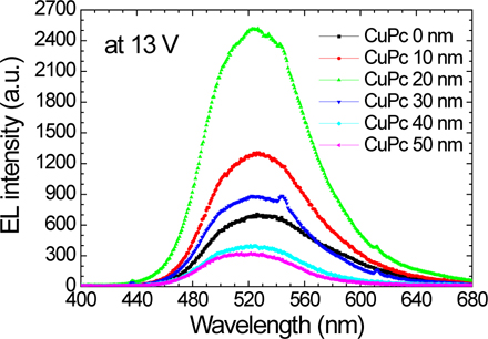
Electroluminescent spectra for the ITO/CuPc (0~50 nm)/TPD/Alq3/Al devices are shown in Fig. 6. All the devices emit a peak wavelength of 530 nm, which is known to be a green light from Alq3. In other words, for Alq3, the emission of light is from the emissive layer. These spectra were obtained by using silicon diode and optical measurement. The results of electroluminescent spectra for the various CuPc thicknesses show that the luminance is higher in the device with 20 nm CuPc layer, and then decrease in the device with 30 nm CuPc layer, showing the consistency of Figs. 3 and 4. We believe that the hole-injecting process would proceed smoothly using a CuPc hole-injection layer, and electroluminescence would reach its maximum value in a device with a 20 nm CuPc layer, at a voltage above 10 V. However, the luminance-voltage characteristics were found to be better in a device with a 10 nm CuPc layer, in the low voltage range of 1~10 V.
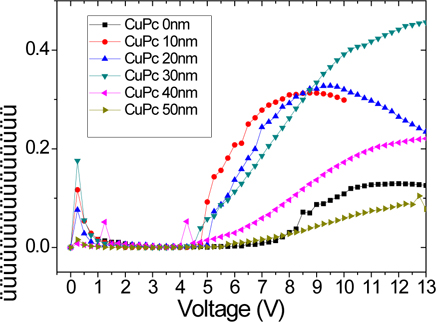
Figure 7 shows the external quantum efficiency-voltage characteristics of the devices with hole-injection layer. The external quantum efficiency of the 10 nm CuPc device is higher at low voltage. Overall, the quantum efficiency of the 30 nm CuPc device exhibits the best characteristics at high voltage. The external quantum efficiency characteristics were obtained from the calculated electroluminescence, and the current-voltage characteristics.
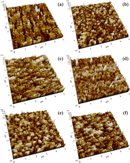
Figure 8 shows the topographies of CuPc layer on an ITO substrate, by using atomic force microscopy (AFM), measured in the non-tapping mode. According to Tadayyon et al., the topography gradually squashes, depending on the increased thickness of CuPc on the bare ITO substrate [5]. In the present study, the results for 0~50 nm thick CuPc are consistent with the tendency reported in the results of Tadayyon et al.
The CuPc layer grows up to 30 nm, and then reaches its maximum value of 40 nm. Above that thickness, the layer is squashed, compared to that of the bare ITO. This result seems to be related to the electrical and optical properties shown in previous figures, and it is thought that the hole-injection is efficient, when the CuPc layer thickness is 10~20 nm.
We have conducted electroluminescent properties of the OLEDs depending on the CuPc hole-injection layer. Devices with CuPc hole-injection layers of 10~30 nm thick exhibit increased luminance. However, the luminance decreases in the device thicker than 30 nm CuPc layer. The devices with CuPc layer show a higher current density that that of the device without holeinjection layer. In addition, low turn-on voltage was achieved in devices with a hole-injection layer, compared to the devices without a hole-injection layer.
The current density-voltage characteristics were investigated in the low and high-voltage range. The external quantum efficiency and electroluminescence exhibit the best characteristics in the device with a 10 nm thick CuPc layer, in the low voltage range of 1~9 V. However, the luminance exhibits the best characteristics in the device with a 20 nm thick CuPc layer, in the high voltage range above 10 V. The external quantum efficiency is the highest in the device with a 30 nm thick CuPc layer, in the high voltage range. However, the external quantum efficiency was appropriate in the device with a 10 nm thick CuPc layer, in the lowvoltage range.
OLEDs with CuPc layer thicknesses of 0~50 nm show that hole injection works most smoothly in the devices with a CuPc layer thicknesses of 10~30 nm. This may be due to the topography of the CuPc layer, and we observed a squashing of the surface morphology, above a certain thickness of CuPc layer. We believe that this squashing interferes with hole injection.