100 nm thick Ga doped ZnO (GZO) thin films were deposited with RF magnetron sputtering on polyethylene terephthalate (PET) and ZnO coated PET substrate and then the effect of the ZnO thickness on the optical and electrical properties of the GZO films was investigated. GZO single layer films had an optical transmittance of 83.7% in the visible wavelength region and a sheet resistance of 2.41 Ω/□, while the optical and electrical properties of the GZO/ZnO bi-layered films were influenced by the thickness of the ZnO buffer layer. GZO films with a 20 nm thick ZnO buffer layer showed a lower sheet resistance of 1.45 Ω/□ and an optical transmittance of 85.9%. As the thickness of ZnO buffer layer in GZO/ZnO bi-layered films increased, both the conductivity and optical transmittance in the visible wavelength region were increased. Based on the figure of merit (FOM), it can be concluded that the ZnO buffer layer effectively increases the optical and electrical performance of GZO films as a transparent and conducting electrode without intentional substrate heating or a post deposition annealing process.
The rapidly increasing use of transparent and conductive oxide (TCO) films such as Sn doped In2O3 (ITO) for heat mirrors [1] and flat panel displays [2] has prompted the development and study of inexpensive TCO materials, which exhibit appropriate optical transmittance and electrical resistivity.
Recently, Al or Ga doped ZnO thin films have been widely investigated as a substitute for ITO due to its low cost, abundance, and non-toxicity [3,4]. Among these elements, Ga is considered one of the most promising since the covalent bonding length of GaO is similar to ZnO when compared to Al [5], which may enable low deformation even at a high doping concentration [6,7]. However, in Ga doped ZnO (GZO) films, relatively high substrate temperatures are required to obtain the necessary electrical resistivity and optical transmittance, simultaneously [8].
One way to improve the optical and electrical properties of GZO films without substrate heating is to use GZO/metal[9], GZO/metal-oxide [10], GZO/metal/GZO [11] structures that have lower resistivity, compared to GZO single layer films of the same thickness.
In this study, GZO films were deposited with radio frequency (RF) magnetron sputtering on polyethylene terephthalate (PET) substrates with and without a ZnO buffer layer and then the effects of a ZnO buffer layer on the optical and electrical properties of the films were investigated by using X-ray diffraction (XRD), atomic force microscopy (AFM), UV-Vis. spectrometry and Hall effect measurements.
GZO single layer and GZO/ZnO bi-layered films were deposited on a PET substrate without intentional substrate heating by RF (13.56 MHz) magnetron sputtering, equipped with two cathodes. The sintered GZO (ZnO 95 - Ga2O3 5 Wt.%, Purity: 99.95%) and pure ZnO (Purity: 99.99%) targets were both 0.25 inch thick and 3 inch in diameter.
During deposition, the substrate temperature was monitored using a K-type thermocouple in contact with the substrate and was found to be constant at about 50℃.
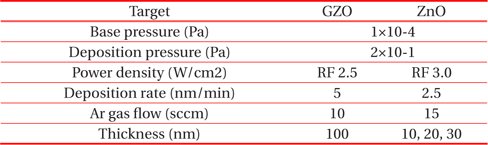
Prior to deposition, the chamber was evacuated to a pressure of 1×10⁻⁴ Pa. Sputtering was performed at 2×10⁻¹ Pa in argon (Ar) and the deposition distance between the target and substrate was maintained at 7 cm. By controlling the deposition time and sputtering power, the thickness of the GZO film was maintained at 100 nm, while the thickness of the ZnO buffer layer was set at 10, 20 and 30 nm, respectively. For comparison, 100 nm thick GZO single layer films were also deposited, under the same deposition conditions. Table 1 shows the deposition conditions of this study.
[Table 1.] Deposition conditions of GZO and ZnO thin films.

Deposition conditions of GZO and ZnO thin films.
After deposition, the crystallization of the films was observed with high resolution X-ray diffraction (XRD, X-pert Pro MRD, Philips, Korea Basic Science Institute, Daegu Center) and the grain size was also evaluated with the Scherrer equation [12]. The root mean square (RMS) roughness was analyzed using atomic force microscopy (AFM, XE-100, Park Systems).
In addition, optical and electrical properties were assessed using four-point probe measurements and a UV-Vis. Spectrophotometer (Cary 100 Cone, Varian), respectively. The PET substrates showed 90% optical transmittance in the visible wavelength range. The performance of the GZO single layer and GZO/ZnO bi-layered films as transparent conducting films was evaluated using the figure of merit (FOM) [13].
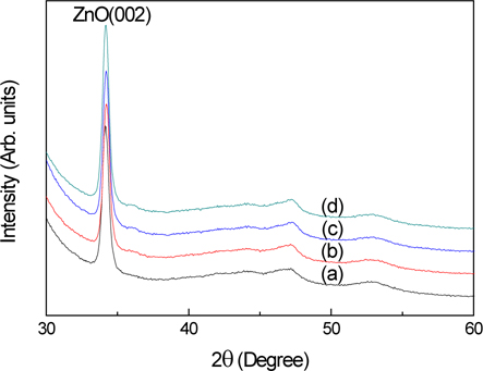
Figure 1 shows the XRD patterns of GZO films with and without a ZnO buffer layer. In order to evaluate the optical and electrical performance of the TCO films, structural characterization is very important because the optical transmittance and resistivity of the films are strongly dependent on the micro-structure.
During deposition, the substrates were not heated intentionally, all the films exhibit a ZnO(002) peak located at 2 θ = 34.14°, indicating that the c-axis is predominantly oriented parallel to the substrate normal. With the increasing thickness of the ZnO buffer layer, the full width at half maximum (FWHM) of the ZnO (002) peak decreased. This means that the crystallization of the GZO film improves with the ZnO buffer layer [10].
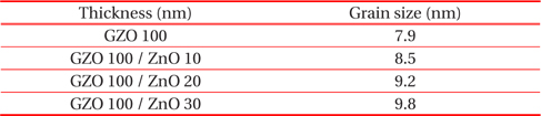
Table 2 shows the grain size of the GZO/ZnO bi-layered films as a function of the ZnO thickness. As the ZnO thickness increases from 10 to 30 nm, the grain size also increases from 7.9 to 9.8 nm. As discussed above, the crystallinity of the film improves as the ZnO thickness increases.
[Table 2.] Comparison of grain sizes of GZO/ZnO bi-layered films as a function of the ZnO thickness.
Comparison of grain sizes of GZO/ZnO bi-layered films as a function of the ZnO thickness.
In a previous study, Kim reported similar results for ITO/Au bi-layered films, the crystallization of the upper ITO film is promoted by an Au buffer layer without intentional substrate heating [14].
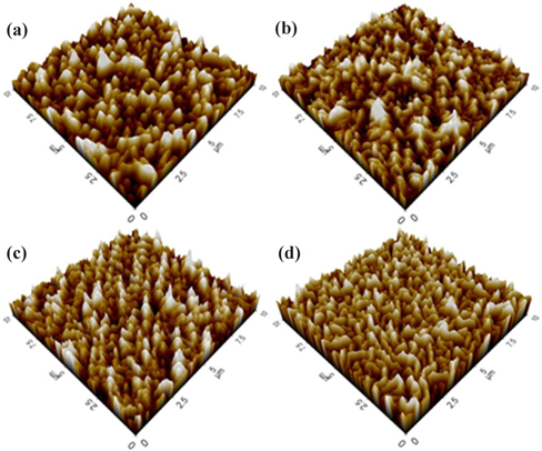
Figure 2 shows the AFM images of GZO single layer and GZO/ ZnO bi-layered films with different ZnO thickness. The RMS roughness of the GZO film (3.3 nm) is lower than that of the GZO/ZnO 30 nm film (4.9 nm).
In a solar cell application, surface roughness of TCO films is a critical factor because the rougher TCO surfaces may allow more optical absorption than flat surfaces. Thus it is supposed that a ZnO buffer layer is effective at enlarging the specific surface area of upper GZO film which is effective on the opto-electrical properties of solar cell applications.
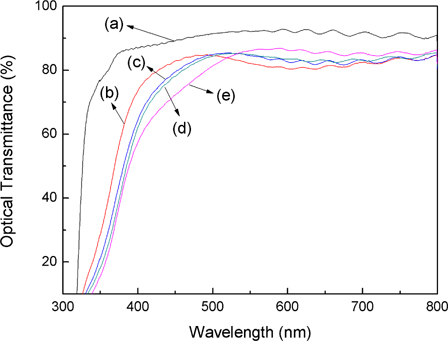
Figure 3 shows the optical transmittance of a GZO single layer and GZO/ZnO bi-layered films for the wavelength range of 300~800 nm. The GZO films show an optical transmittance of 83% and as the thickness of the ZnO buffer layer increases, the optical transmittance of the films is also increased. The GZO 100 nm/ZnO 10 nm, GZO 100 nm/ZnO 20 nm and GZO 100 nm/ZnO 30 nm films show the higher optical transmittances of 85.5%, 85.9 and 86.2%, respectively, more than that of the GZO single layer films.
As shown in Figure 3, the increment of the optical transmittance of GZO/ZnO bi-layered films is thought to be due to the enhanced crystallization of the GZO/ZnO films because the grain boundary acts as an optical absorption source in TCO films [15].
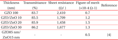
Table 3 shows the evaluated figure of merit (FOM) in this study [16]. The FOM is defined as FOM = T10/Rs, where T is the average optical transmittance in the visible wavelength region and Rs is the sheet resistance of the films. The FOM reached a maximum of 1.5×10⁻⁴ Ω-1 for the GZO 100 nm/ZnO 20 nm films. Since a higher FOM value means better quality TCO films, it is concluded that the optimized ZnO buffer layer enhances the optical and electrical properties of the GZO films [12].

The figure of merit of GZO single layer and GZO/ZnO bilayered films with different thickness of ZnO buffer layer (thickness of GZO film ; 100 nm).
Both GZO single layer and GZO/ZnO bi-layered films were deposited with RF magnetron sputtering on PET substrates and then the influence of the thickness of the ZnO buffer layer on the optical and electrical properties of the GZO films was investigated.
The figure of merit for the GZO 100 nm / ZnO 20 nm films reached a maximum value of 1.5×10⁻⁴ Ω-1, which is higher than that of the GZO single layer films. Since the higher FOM value indicates better performance of TCO films, it is thought that the GZO films with 20 nm thick ZnO buffer layers will likely perform better in TCO applications than GZO single layer films.