ZnO-based semiconductors are attractive for various applications such as optoelectronic devices, solar cells, flat panel, and flexible display applications because they have higher electron mobility than amorphous silicon, a wide direct band gap of 3.37 eV at room temperature, and high exciton binding energy of 60 meV. ZnO with wurtzite structure has a large exciton binding energy of 60 meV, which operates at room temperature, and enlarges its efficiency. However, the presence of defects in the ZnO-related materials affects the electrical and optical properties, degrading the performance and efficiency [1-3]. Generally, ZnO exhibits ultraviolet emission caused by the free exciton recombination, accompanying a broad visible emission. In order to fabricate highly efficient optoelectronic devices, the origin of deep level emissions observed in the visible region should be clearly defined. The deep level (DL) emissions due to defects in the ZnO-related materials consist of orange-red (2.28 eV) and green (2.45 eV) emissions in the visible region, and blue (2.85 eV) and violet (3.1 eV) emissions in the near UV regions [4,5]. The transition energy from Zn interstitials (Zni) level to the valence band in ZnO corresponds to 3.1 eV. The green and orange-red emissions were attributed to oxygen vacancies (Vo) and oxygen interstitials (Oi), respectively [6]. The presence of Vo as electron donor induces electric conductivity in ZnO grown on SiN or SiO2 prepared by the Sputtering method. But the yellow emission at 580 nm in ZnO has been associated with electron acceptor defects, such as Oi. A high concentration of electron acceptor defects in ZnO is related to large threshold voltage (ΔVth) in thin film transistors (TFTs) and low electron mobility [7,8]. Hence it is necessary to study the suppressed defect-related emissions, in order to fabricate highly efficient devices. Numerous studies have been conducted on blue and green emissions with ZnO-related thin films that are deposited on various substrates at different RF powers. The growth of ZnO on Si also involved defects due to the Si-O bond and the large lattice mismatch between Si substrate and ZnO film. Thus, the discovery of substrate materials to improve the crystallinity of ZnO-related oxides has been researched. The sputter deposition of ZnO-type thin film should be performed at low temperature because of the deformation of the film properties through degradation at high temperature [9-11]. SiOC is a promising low-k (low dielectric constant) material that can replace SiO2 film. It has been known that the dielectric constant of SiOC film fabricated by CVD (chemical vapor deposition) decreases as the polarization of the film lowers. Moreover, it has been reported that SiOC as a gate insulator improves the performance of TFT [12]. The electron emission of the defects resulting from the localized deep level states in semiconductor band gap is associated with the ionization energy of the localized state in dielectric materials. In other words, the localized trap barrier or deep level emission is related to its ionization energy, because the charge carriers in semiconductors originate from the impurities or defects. To understand the state of defects in semiconductors, the Mitrofanov group suggested an Arrhenius plot describing the defects, which shows that the intensity of the emission is inversely proportional to the value of the ionization energy (Ei). Usually, the Arrhenius plot was treated with high-k materials [13].
In this study, to observe the correlation between the ionization energy and the deep level emission state of SiOC, the characteristic of SiOC was analyzed, by using PL spectra at various RF powers. The ionization energy comes from the potential barrier, where an arrested charge carrier departs from a localized state to a free state, and the emission is associated with the correlation between the potential barrier and dielectric constant of SiOC films. To research the interface between the active layer and dielectric, AZO thin films on SiOC film were grown with increasing RF power by an RF magnetron sputter system, and the effects of the optical properties of the AZO thin films were investigated. The origins of deep level emissions due to the defects in AZO films were studied.
In order to study the emission characteristic of ZnO-based materials, AZO thin film was deposited on SiOC/n-type Si wafers by RF magnetron sputtering at a pressure of 0.01 Torr under argon atmosphere. AZO targets (99.99% purity) were supplied by LTS Research Laboratories, Inc., U.S.A. The base pressure was 4.5 × 10⁻⁵ Pa. The flow rate of the argon (99.9999%) was controlled by a mass flow controller (MFC) at 30 sccm, and the sputtering RF power ranged from 50 to 200 W. AZO film on SiOC/Si was prepared at room temperature. SiOC films were formed by inductively coupled plasma-chemical vapor deposition (ICPCVD) using the gas flow rates of 5 sccm: 5 sccm with oxygen and dimethyldimethoxysilane (DMDMOS), and the detailed preparation method is explained in previous studies [4,14]. Chemical-optical analysis of the film was performed by using photoluminescence (PL) spectrometry. PL spectra were obtained by UV-visible spectrometer with xenon lamp as a light source, at the High Technology Components & Materials Research Center, South Korea. The roughness was observed by atomic force microscopy (AFM, S.I.S., GmbH at Cheongju University). The emission and structural properties of the AZO film on SiOC film were investigated from the results observed by the PL analyses and AFM images.
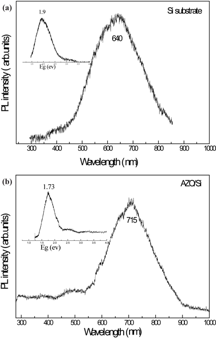
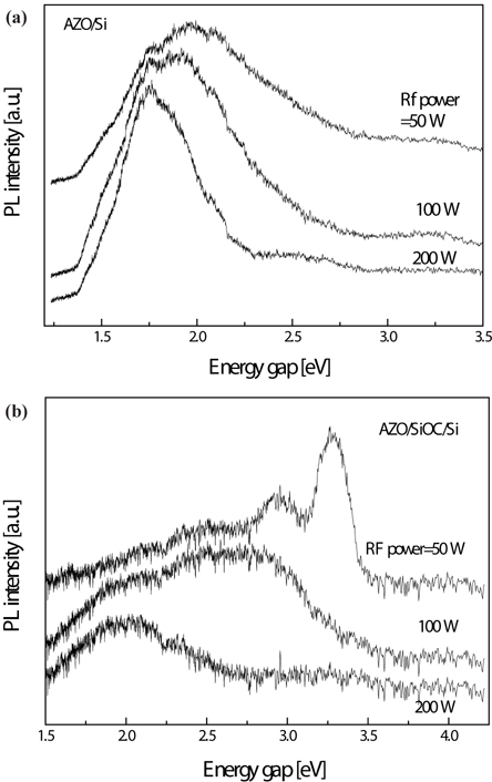
To characterize the substrate during AZO growth, it has to be taken into account that the particles are in a certain range of energy to reach the surface of the substrate for the growth on substrate. The PL spectra of Si wafer and AZO/Si film are analyzed in Fig. 1. The energy gap of Si wafer in Fig. 1(a) is 1.9 eV and the shape of PL signal peak centered at 640 nm is broad. Following AZO deposition with the RF magnetron sputter, the central peak of PL signal moves to a higher wavelength of 715 nm, and the energy gap decreases to 1.73 eV. The strong red emission is due to a recombination of excitons in the surface region of Si. The weak green and orange-red emissions in the visible range can be attributed to native defects in AZO and to an oxygen bond with Si wafer [4].
In order to study the visible emissions caused by various defects in Al-doped ZnO layer, the Al-doped ZnO layers were grown on n-type Si substrates and SiOC/Si film by RF-magnetron sputtering. SiOC film was prepared by inductively coupled plasma chemical-vapor deposition (ICP-CVD) using the gas flow rates of 5 sccm: 5 sccm with oxygen and dimethyldimethoxysilane (DMDMOS). To analyze the high-energy particles reaching the substrates, the PL spectra of the AZO films were measured.
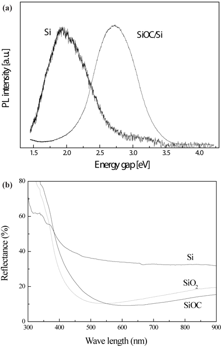
Figure 2(a) shows the energy gap of Si wafer and SiOC/Si film. The energy gap of SiOC grown on Si wafer film is higher (2.8 eV) than that of Si wafer (1.9 eV). The amorphous SiOC film has large energy gaps, due to the attractive forces between an electron deficient carbon and a highly electronegative oxygen. Moreover, the SiOC film is a good insulator of low dielectric constant. PL spectra of 1.9~3.6 eV signify the typical emission of SiOC film on Si wafer in the UV and visible region [5,13]. The PL spectra of Si wafer consist of the orange-red region (1.75 eV), and yellow region (2.2 eV). However, the PL spectra of SiOC/Si film consist of blue (2.85 eV), and violet (3.25 eV). To compare the optical properties of Si, SiO2, and SiOC films, the reflectance was also measured. The reflectances of SiO2 and SiOC films are similar, and that of SiOC is almost two to three times lower in the visible range than the reflectance of Si wafer, as shown in Fig. 2(b), indicating that the absorption and emission of SiOC in the visible range occur more actively, than those of Si. Usually, ceramics such as SiOC and SiO2 show lower reflectance values, compared with a semimetal like Si.
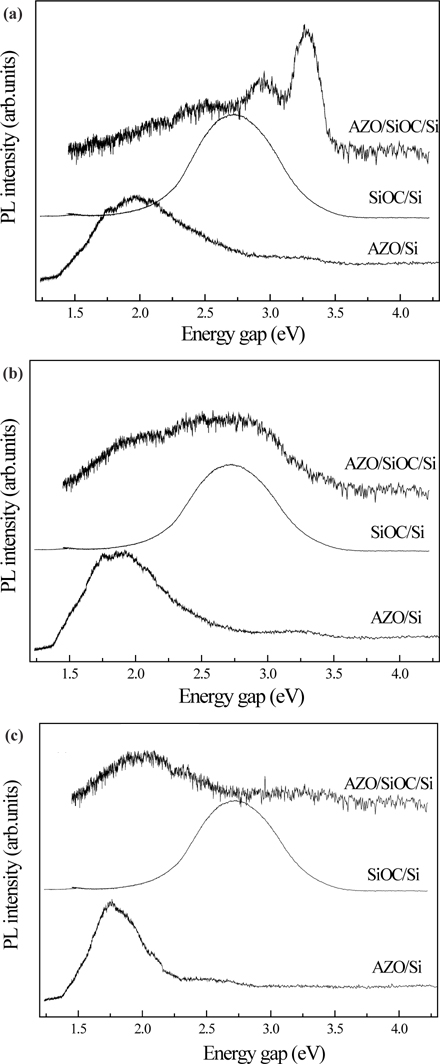
In Fig. 3(a), the PL measurements for AZO layers on Si substrates were first carried out, to examine the deep level (DL) emissions with increasing RF-power. AZO layer grown on Si showed broad DL emission in the orange-red region (1.75 eV) and yellow region (2.2 eV) under pure Ar atmosphere, and the phase behavior shifted towards a higher energy gap, as the RFpower decreased. The peaks were 1.75, 1.9, and 2.0 eV, at RFpower of 200, 100, and 50 W, respectively. The orange-red and yellow emissions in the visible range are attributed to native defects in AZO. When the RF-power increases, the quantum energy based on the defects between AZO film and Si wafer decreases.
Figure 3(b) shows the DL emissions of AZO films prepared on SiOC/Si film at different RF-power. It is estimated that the difference in optical property compared with Fig. 3(a) results from the different characteristics of the substrates, Si and SiOC/Si films. The results observed from the PL spectrum in the range 1.4~3.5 eV indicate that various defects exist. The deep level emission across the visible light region is attributed to the diversity of structural defects, such as oxygen vacancies, zinc interstitials, and free carriers formed by Aldoping.
The energy gap obtained from the chemical shift increases with decreasing RF-power, indicating an improvement of the crystallinity of the AZO film at low RF-power. The recombination of ionized sites is activated with decreasing RF-power, and then the emission progresses towards the UV emission range. The DL emissions in the visible region might also be due to the energy level formed by impurities or Al-doping. The visible emission observed in ZnO-based films generally originates from various intrinsic defects, such as Zni, Vo, VZn, and Oi. Recent studies on the DL emission of ZnO have demonstrated that the green emission at 2.5 eV is related to oxygen vacancies, and the red emission at ~2 eV is related to oxygen interstitials or excess oxygen [4]. In the dominant defects for the ZnO-based materials, the orangered emission is usually observed in an oxygen-rich atmosphere, together with the increment of numbers of oxygen interstitial defects in AZO film. On the other hand, the green emission in oxygen-deficient sample might be due to the Vo. The orange-red emission is dominant with increasing RF-power at AZO on SiOC film, as shown in Fig. 3(b). The oxygen-rich ambient condition under high RF-power generates structural defects, like Oi in AZO film. However, the oxygen ions in oxygen-deficient region at low RF-power improve the crystallinity of AZO film, and generate blue (2.85 eV) and violet (3.25 eV) emissions, owing to the increase of energy gap. The PL spectra of AZO/SiOC/Si film at low RF-power consist of orange-red (1.75 eV), yellow (2.2 eV), green (2.5 eV), blue (2.85 eV), and violet (3.25 eV) regions. The increase in the number of intrinsic defects, such as Zni (2.85 eV) and Vo (2.5 eV), enriches the background electron concentration and oxygen vacancy related emission [5].
The sample at RF-power of 200 W shows an intense orangered emission, which implies an oxygen rich growth condition. The orange-red emission is attributed to a decrease in quantum energy, due to the defects generated by RF power energy during the deposition. The sample at RF-power of 100 W involves the broad band emission from 1.4 to 3.5 eV, with defects of Oi (2.2 eV), Vo (2.5 eV), and Zni (2.85 eV). However, the sample at RFpower of 50 W shows blue (Zni, 2.85 eV) and very strong violet (VZn, 3.25 eV) emissions near the UV region. ZnO-based films grown in the oxygen deficient condition increase the electric conductivity, and improve the crystallinity. Compared with the band gap of AZO grown on Si at the same RF-power condition, it was also found that the optical band gap of AZO grown on SiOC increases due to the appropriate matching between AZO and SiOC films, and due to the different characteristics between SiOC and Si.
Both Figs. 3(a) and (b) show that the emissions move to a high energy gap with decreasing RF-power. When the sputtering RF power is applied, the high-energy particles reach the surface of Si or SiOC/Si substrate for growth on the substrate. When the RF-power is high enough, all the particles with higher energy impact strongly on the substrate; then some particles bounce off of the substrate, while the others strongly adsorb onto the substrate which mainly induce the orangered emission. When low RF-power is applied, the particles with lower energy impact on the substrate, then most of the particles adsorb onto the substrate with various strength, and only a few particles bounce off of the substrate, which produces diverse defects depending on the degree of adsorbed strength on substrate, forming the characteristic interface between AZO and the substrate. Therefore, as shown in both Figs. 3(a) and (b), the emissions shift to a higher energy gap as RF-power decreases. In particular, the interface between AZO film and SiOC/Si substrate contributes to an increased energy gap near the UV region, by the diversity of defects at low RF-power. This means that the control of the RF-power in the sputtering process is very important in obtaining blue region emissions from AZO grown on SiOC film.
To examine the origin of DL emission in more detail, substrate-dependent PL measurements were performed, as shown in Fig. 4. Considering the variation of RF-power used in sputtering, DL emissions in the visible region are attributed to the diversity of structural defects such as oxygen vacancies, zinc interstitial, and free carriers formed by Al-doping. Figure 4 shows that the blue and violet emissions of AZO/SiOC/ Si film at RF-power of 50 W are dominant depending on the characteristic of interface between AZO and SiOC film. This indicates that violet and blue emissions are responsible for the defect states of VZn and Zni in Al doped ZnO-related thin film. Figure 4 shows the chemical shift resulting from a carrier localization effect, with increasing RF-power. The carrier localization arising from the oxygen rich sites at high RF-power decreases the quantum energy, and then causes red shift from blue emission. The 3.1 eV peak in the violet region at RFpower of 50 W is due to band transition from the Zni level to the valence band. Moreover, it has already been mentioned that the orange-red and yellow emissions move to higher energy with decreasing RF-power at AZO/Si film as shown in Fig. 4(a). It was also observed that the violet emission disappeares at RF power of 200 W, as shown in Fig. 4(c). The growth of AZO film under excess oxygen gas at high RF-power generates oxygen interstitial sites. Generally, high quality ZnO should have a high crystalline ordering for high emission efficiency. The degree of crystallization in ZnO films has a strong influence on device performance. The PL peak shape of AZO/SiOC/Si thin film becomes a generally broad peak with increasing RF-power, but the PL of a sample prepared at a low RF-power of 50 W shows strong violet and blue emissions near the UV region. Hence, the crystallinity of AZO film grown on SiOC formed at 50 W is also improved.
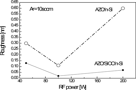
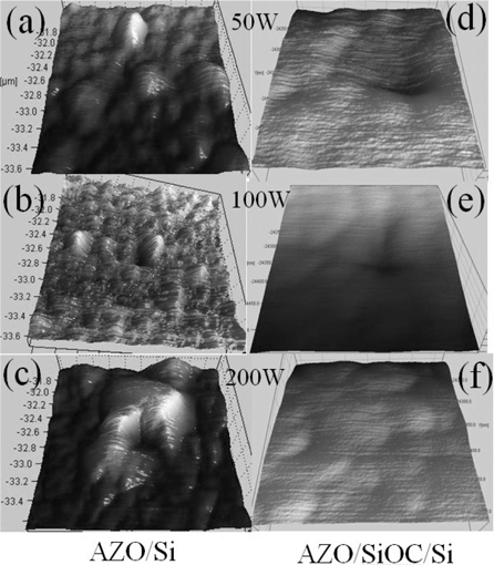
Figure 5 shows the AFM images of AZO on Si and SiOC/Si substrates with increasing RF-power. Figs. 5 (a), (b), and (c) are images of AZO prepared on n-type Si, and Figs. 5(d), (e), and (f ) are the results of AZO on SiOC films, which were fabricated at various RF powers of 50, 100, and 200 W. AFM images of AZO grown on SiOC/Si substrates show flat surfaces in comparison with AZO grown on Si wafer.
Figure 6 shows the roughness of AZO films deposited on Si and SiOC/Si substrates. The roughness is influenced by the amount of defects in localized trapped states, and localized donor states are located on the surface of the semiconductor. Generally, amorphous SiOC reduces the localized trapped states produced from defects in the AZO, enhances the surface flatness by low surface ionization energy, and decreases the roughness. When the number of defects increases, the energy gap increases, depending on the excitons captured at the localized trapped states. The behavior of excitons in SiOC can be improved, by controlling RF power for AZO deposition. The shift to the high energy gap of SiOC as an insulator, as seen in Fig. 2(a) results in the flat surface. The roughness decreases when the localized state produced from defects has low surface ionization energy at low power. On the other hand, the roughness of surface increases at high RF-powers, although the AZO deposited on SiOC/Si wafer at low RF-power of 50 W has comparatively high roughness, showing a different roughness pattern from the others. However, it has already been described that the crystallinity and the energy gap of AZO/SiOC/Si increases at a low RF-power of 50 W, as shown in Fig. 4(a), where high emission efficiency for device performance in the blue and violet regions can be obtained.
These results indicate that the lowering of polarization of SiOC film enhances the growth of AZO, and amorphous SiOC film reduces the mismatch between AZO layer and Si wafer. The low dielectric property of SiOC film is based on the decrease of polarization between the hydroxyl and alkyl functional groups, during the CVD-deposition. In particular, the dielectric performance is superior to the conventional SiO2 dielectric film, because low dielectric SiOC (εr ≈ 2.1) based on amorphous structure has the advantages of low power consumption and no cross talk [14]. The formation of flat surface in AZO grown on amorphous SiOC improves the physical-electrical performance, by reducing the mismatch generated at the interfaces.
To explore the interface effect between as-deposited AZO and SiOC film, AZO thin films were prepared on SiOC film by RF-magnetron sputtering at various RF-powers, and analyzed by optical characteristics, using the PL spectrum. The deep level emissions across the visible light region of a AZO/SiOC film are attributed to the diversity of structural defects, such as oxygen vacancies, oxygen interstitials, zinc vacancies, zinc interstitials, and free carriers formed by Al-doping. The roughness of AZO deposited on SiOC decreases and its flatness is improved, because of the matching effect of SiOC between a ZnO-based film and Si substrate. Thus the energy gap increases when AZO is deposited on SiOC. Moreover, AZO prepared at low RF power shows a high energy gap, depending on the formation of an amorphous structure. The RF-power as an activation energy for chemical reaction is related to the crystallinity of the ZnO wurtzite hexagonal phase. Consequently, it can be estimated that the ZnO-based thin films deposited on SiOC/Si substrate at room temperature are useful in various potential applications such as solid white light sources, solar cells, and LED devices with high efficiency.