Pt/Al2O3/La2Si5Ox/SiO2/Si charge trap memory capacitors were prepared, in which the La2Si5Ox film was used as the charge trapping layer, and the effects of post annealing atmospheres (NH3 and N2) on their memory characteristics were investigated. La2O3 nanocrystallites, as the storage nodes, precipitated from the amorphous La2Si5Ox film during rapid thermal annealing. The NH3 annealed memory capacitor showed higher charge storage performances than either the capacitor without annealing or the capacitor annealed in N2. The memory characteristics were enhanced because more nitrogen was incorporated at the La2Si5Ox/SiO2 interface and interfacial reaction was suppressed after the NH3 annealing treatment.
With conventional floating gate type memories approaching their scaling limit, tremendous effort has been made to explore next generation nonvolatile memory devices [1-5]. Of the alternatives, nanocrystallite (NC)-based charge trap memory (CTM) devices have received much attention in the electronics industry because of their advantages such as lower operation voltage, higher endurance, and simple fabrication process compatible with standard complementary metal oxide semiconductor (CMOS) technology [6-9]. Numerous works have focused on developing charge trapping layers containing metallic or semiconducting NCs for use in nonvolatile memory devices [10-17]. However, researchers have been challenged by the poor thermal stability as well as the incompatibility with the metal oxide semiconductor (MOS) process of metallic or semiconducting NC memory devices [18,19].
In this work, we report enhanced charge trap memory characteristics by precipitation of NCs from the amorphous La2Si5Ox (noted as LSO) charge trapping layer through rapid thermal annealing (RTA). In addition, the effects of post annealing in different atmospheres (NH3 and N2) on the memory characteristics of memory window and data retention are reported in this paper.
La2O3 NC-based CTM capacitors with a Pt/Al2O3/LSO/SiO2/ p-Si stack structure were fabricated. Prior to film deposition, p-type Si (100) substrates with a resistivity of 3~20 Ω·cm were cleaned by the standard Radio Corporation of America (RCA) process to remove native oxide. Then, 3 nm SiO2 was thermally grown in dry O2 at 900℃ as the tunneling layer. An LSO charge trapping layer of ~6 nm thickness was deposited by pulsed laser deposition (PLD) at a substrate temperature of 350℃. Subsequently, 8 nm Al2O3 was deposited as the blocking layer by atomic layer deposition (ALD) using tri-methylaluminium (Al(CH3)3) precursors at a substrate temperature of 300℃. The fabricated memory device without post annealing was denoted as S1. After the above processes, the memory capacitors were rapid -thermal - annealed at 900℃ for 30 s in N2 and NH3 atmospheres, and were denoted as S2 and S3, respectively. Finally, platinum (Pt) gate electrodes (7.85×105 cm2) with a patterned mask were deposited on the blocking layer by the magnetron sputtering technique at room temperature. The thermal stability of the LSO films was examined by X-ray diffraction (XRD) and X-ray photoelectron spectroscopy (XPS), and the cross sections and interface quality of the memory capacitors were revealed in highresolution transmission electron microscope (HRTEM) images. The electrical characteristics of the memory capacitors were measured using a Keithley 4200 semiconductor characterization system (4200 SCS).
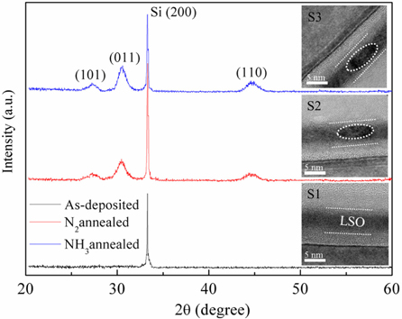
The XRD patterns of as-deposited and RTA - treated LSO films are presented in Fig. 1. The as-deposited LSO films remain amorphous, but some crystalline peaks appear after RTA at 900℃ in N2 and NH3 atmospheres. These diffraction peaks correspond to the (101), (011) and (110) planes of cubic La2O3 [20], respectively. The results show that the crystalline La2O3 phase precipitated from the amorphous LSO matrix after RTA treatment. The inset of Fig. 1 shows the cross sectional HRTEM images of the S1, S2 and S3 samples, respectively. The La2O3 NCs, as indicated by the dotted circles, precipitated and became embedded in the LSO film matrix after the N2 and NH3 annealing treatments.
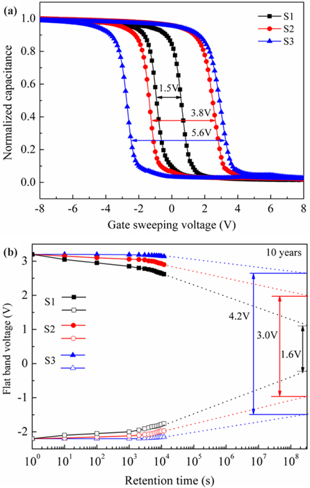
Figure 2(a) illustrates the high frequency (1 MHz) capacitancevoltage (C-V) hysteresis memory windows of the memory capacitors, measured under the same gate sweeping voltage. Memory window is defined as the difference in the flat band voltages between the program and erase states. The hysteresis memory windows of the S1, S2 and S3 samples were measured to be 1.5 V, 3.8 V, and 5.6 V, respectively. We programmed the above three memory capacitors to have the same initial flat band voltage (5.4 V) to compare their data retention characteristics at room temperature, as shown in Fig. 2(b). The charge losses of the S1, S2 and S3 samples were 15%, 10% and 2% after 1.2×10⁴ s, respectively. In order to predict the long-term charge retention characteristics of the samples, the experimental results were extrapolated; the charge losses of the S1, S2 and S3 samples after 10 years would be 70%, 44% and 22%, respectively, which suggested that the N2 and NH3 annealing treatments could reduce the charge loss. The S3 has the optimum retention performance, which may be due to the nitrogen incorporation at the La2Si5Ox/SiO2 interface and the effective suppression of interfacial reaction after the NH3 annealing treatment, as discussed below.
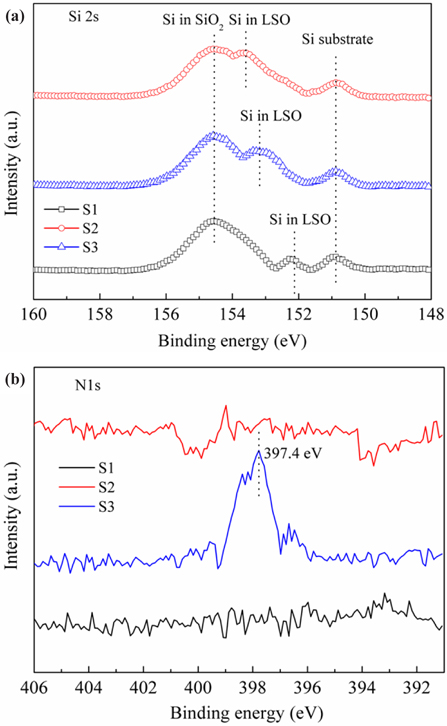
To determine the effect of annealing atmosphere on memory characteristics, the LSO/SiO2 interface before and after annealing treatment was evaluated by XPS analysis. Figure 3(a) shows the XPS spectra of the Si 2s for the S1, S2 and S3 samples, respectively. For the S1 sample, the peak located at 150.9 eV corresponds to the Si substrate, while the peaks located at 152.3 and 154.6 eV correspond to La-silicate and SiO2, respectively. The weak La-silicate peak intensity means that there is no obvious interfacial layer at the LSO/SiO2 interface before annealing. For the S2 and S3 samples, however, the intensity of the La-silicate peak increases, suggesting interfacial reaction at the LSO/SiO2 interface during the post annealing process [21]. Moreover, the La-silicate peak position shifts to the high binding energy position, indicating that the Si content increases at the LSO/SiO2 interface to form Si rich La-silicate. For the S3 sample, the relatively weaker La-silicate peak intensity indicates that NH3 annealing can suppress interfacial reaction, unlike N2 annealing. In addition, the binding energies of the La-silicate peaks of the S2 and S3 samples are 153.7 and 153.3 eV, respectively. The lower binding energy of the S3 sample may be due to the presence of nitrogen in the film [22-25]. Figure 3(b) shows the N 1s XPS spectra of the S1, S2 and S3 samples, respectively: the N 1s peak of the S3 sample is at 397.4 eV, but those of the S1 and S2 samples cannot be observed. The results indicate that NH3 annealing can effectively incorporate nitrogen at the LSO/SiO2 interface, suppress interfacial reaction, and decrease charge loss to enhance memory performance. Therefore, a La2O3 NC - based CTM device after NH3 annealing is a promising candidate for future nonvolatile memory applications.
We fabricated charge trap memory capacitors with a Pt/Al2O3/ La2Si5Ox/SiO2/Si stack structure, in which the La2Si5Ox film was used for charge trapping. The effects of post annealing atmospheres (NH3 and N2) on their charge memory characteristics were investigated. The La2O3 nanocrystallites, as the storage nodes, precipitated from the amorphous La2Si5Ox film during rapid thermal annealing. The NH3 atmosphere annealed memory capacitor showed higher charge storage performance (i.e., larger memory window and optimal data retention) than either the capacitor without annealing or the capacitor annealed in N2, This result could be due to the more nitrogen incorporation at the La2Si5Ox/SiO2 interface and the effective suppression of interfacial reaction after the NH3 annealing treatment.