In this paper, metal insulator metal (MIM) plasmonic slot cavity narrow band-pass filters (NBPFs) are studied. The metal and dielectric of the structures are silver (Ag) and air, respectively. To improve the quality factor and attenuation range, two novel NBPFs based on tapered structures and double cavity systems are proposed and numerically analyzed by using the two-dimensional (2-D) finite difference time domain (FDTD) method. The impact of different parameters on the transmission spectrum is scrutinized. We have shown that increasing the cavities’ lengths increases the resonance wavelength in a linear relationship, and also increases the quality factor, and simultaneously the attenuation of the wave transmitted through the cavities. Furthermore, increasing the slope of tapers of the input and output waveguides decreases attenuation of the wave transmitted through the waveguide, but simultaneously decreases the quality factor, hence there should be a trade-off between loss and quality factor. However, the idea of adding tapers to the waveguides’ discontinuities of the simple structure helps us to improve the device total performance, such as quality factor for the single cavity and attenuation range for the double cavity. According to the proposed NBPFs, two, three, and four-port power splitters functioning at 1320 nm and novel ultra-compact two-wavelength and triple-wavelength demultiplexers in the range of 1300-1550 nm are proposed and the impacts of different parameters on their performances are numerically investigated. The idea of using tapered waveguides at the structure discontinuities facilitates the design of ultra-compact demultiplexers and splitters.
Modern electronic devices are rapidly approaching their fundamental speed and bandwidth limitations, creating a serious impediment for new applications and requirements. Carrying information by light and replacing electronic signals by lightwave is an auspicious solution towards higher speeds. The diffraction limit prevents the localization of light in areas smaller than a wavelength; therefore, miniaturization and integration of conventional photonic circuits are impossible [1]. Excitation of surface plasmons is one of the most feasible ways to guide electromagnetic waves beyond the diffraction limit to control light in the nanometer scales. Estimations show that data rates of 10 Tbit/s are achievable by decreasing the photonic devices to subwavelength scales [2].
A plasmon is a quasi-particle and quantum of plasma oscillation of free electrons in a metal. Plasmons with collective electron oscillations confined to the interface of metal and dielectric are called surface plasmons (SPs). When a photon (a quantum of electromagnetic wave) is coupled to a SP, the quasi-particle known as the surface plasmon polariton (SPP) is produced. SPPs are surface electromagnetic waves propagating along the metal-dielectric interface and are evanescently confined in the perpendicular direction of the interface. In a cylindrical metal nanowire, when the diameter is reduced below the light wavelength, a strong monotonic increase in localization of light takes place and shows that the diffraction limit can be overcome [2].
Different metallic plasmonic nanoguiding structures including thin metal films, metal nanorods, metal wedges, nanogrooves, slot waveguides, etc. have been proposed and their properties have been studied [1]. Two of the well-known multilayer plasmonic waveguides are metal-insulator-metal (MIM) and insulator-metal-insulator (IMI) structures. MIM structure gives more light confinement, but more propagation loss (lower propagation length). Therefore, there should be a tradeoff between propagation length and light confinement. It is shown that MIM structure is a superior choice [3]. It is also experimentally verified that silver, due to its lower guiding loss, is an appropriate metal for plasmonic waveguides [4].
To realize photonic circuitry based on plasmonics, a variety of components such as splitters [5-7], couplers [8, 9], multi-demultiplexers [10-13], switches [14], logic gates [15], etc. have recently been studied. Filters as a fundamental block, have been at the center of attention. Filters can be divided into three categories of narrow band-stop filters (NBSFs) including fiber Bragg gratings, Fabry-Perot and slot filters [2, 8, 10, 16-24], narrow band-pass filters (NBPFs) [10, 17, 11, 20, 25-30], high-pass [31], and low-pass (cutoff) [32] filters, which have been widely studied.
One of the most important characteristics of these filters (NBPF or NBSF), is their quality factor, defined as
Using filters as a fundamental block, different splitters such as one in [26], based on slot cavity filters and several plasmonic demultiplexer structures have been proposed. A plasmonic demultiplexer based on a Y bent waveguide is presented, but it needs a minimum space of 2μm between the input and the outputs, which may not be desirable for compact circuitry [10]. In [12], a nano-plasmonic triple-wavelength demultiplexer is presented, but due to the weak coupling effect, the resonance frequencies are not transmitted properly and corresponding spectrum peak values are undesirably low. Tao
In this paper, we begin with an in-line cavity NBPF structure and based on tapered waveguides, we modify it to yield two novel slot cavity NBPF structures with two different perspectives. Both have an acceptable spectrum peak value. We are trying to obtain a relatively high quality factor filter with one of them and a filter with a high attenuation range with the other one. High attenuation range helps to damp the undesired frequencies around the resonance. Then, based on the proposed filters, a novel splitter and compact demultiplexer are proposed. The demultiplexer is around 900nm long and 350nm wide. The structures are numerically studied.
The paper is organized as follows; in Section II some introductory concepts of plasmons and the FDTD method are discussed. In Section III, the structures proposed are simulated. The paper is concluded in Section IV.
II. SURFACE PLASMON POLARITONS AND METHODS FOR THEIR ANALYSIS
The surface plasmon is a classic electromagnetic topic, known from 100 hundred years ago, but, due to the recent advances in nanotechnology, it has become an interesting topic of research for scientists [35]. At optical frequencies, metals can be described by a gas of free electrons moving against a positive background of ion cores, which are known as the plasma model. In response to an applied electromagnetic field, the electrons oscillate and their motion is damped with a characteristic collision frequency of
where

where
In this paper, we have used the silver parameters of:
[TABLE 1.] Parameters of the Drude-Lorentz model for silver [25]

Parameters of the Drude-Lorentz model for silver [25]
Solving the Helmholtz equation and applying boundary conditions, show that SPPs exist only for TM modes. This is due to the negative real part of the dielectric function of metal at optical frequencies [36]. However, lightwaves cannot directly excite the SPPs in normal conditions, because the photons’ momentum is lower than that of the SPPs. Some exciting techniques such as prism coupling, scattering from a topological defect, and using periodic corrugations in the metal’s surface are required to match the momentum. Once light is coupled to SPPs, it will be propagated along the interface and will also be attenuated accordingly [35].
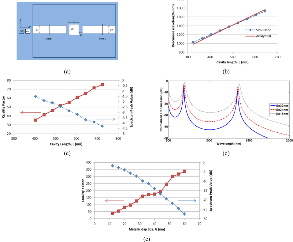
The schematic view of a typical MIM waveguide, with an in-line slot cavity is shown in Fig. 1. The incident wave is either reflected from or coupled to the cavity. Constructive reflections inside the slit at a specific wavelength form standing waves and the structure operates as a resonance device. Therefore, the incident wave is passed or blocked and the total structure operates as a NBPF. To find the empirical relation for the resonance wavelength, the condition for constructive interference is required. Based on the principle of a resonant cavity, the necessary condition for the case is that the phase delay per round trip in the cavity to be an even multiple of

where

The effective refractive index is a function of waveguide width and the operating frequency. Using International Mathematics and Statistics Library (IMSL) Fortran subroutine,
To simulate the plasmonic filters, we have used the FDTD method in which Maxwell’s equations are solved by discretizing time and space. The spatial grid size is Δ
The numerical calculations are convergent for the number of time steps of up to 220. A very important point to be noticed is the distance of the source from CPML layers, which should be far enough to converge the numerical calculations. We have found that the distance of 1μm is required to avoid instability of the numerical simulations.
3.1. Narrow Band-pass Filter Structure
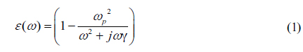
The first structure to be analytically and numerically investigated is depicted in Fig. 1(a). The in-line resonator cavity with length L and width W operates as a narrow band-pass filter, and it only passes the cavity resonance wavelength. We are interested in the impact of the parameters of the cavity on the transmission spectra. We have mostly focused on the wavelengths longer than 1 μm. Though other modes may appear, we have concentrated on the fundamental mode to be appropriate for the second and third telecommunication windows. For more accuracy, we have calculated the input power without metallic gap to eliminate the cavity reflection effects. Therefore, for each graph we have run the codes two times, with and without the metallic gap and resonator cavity. The results are depicted in graphs of Fig. 1 and Table 2. The important data, quality factor, spectrum peak value and resonance wavelength in Table 2 are derived from the simulated band-pass filters for easier quantitative evaluations. The structure of Fig. 1(a) has been studied in some other references [10], [17], but the wavelength spectrum and dielectric medium are not the same, so for an exact analysis and comparison of the presented modified structures with the NBPF structure, we have chosen air as the dielectric and wavelengths above 1 μm as our simulating spectrum. Three important results should be noticed:
a) Increasing the cavity length increases the resonance wavelength in a linear relationship, which complies with the analytical results for resonance wavelength of Eq. (4). As shown in Table 2, the numerical and analytical results for λr as a function of L are approximately the same. It is also observed that increasing L, would increase Q, but decreases the spectrum peak value. b) Increasing the width of the cavity, W, enhances the filter quality factor, but decreases the spectrum peak value. Furthermore, the resonance wavelength is slightly decreased. The change in λr for the same length is the effect of change in ϕref and effective index which slightly changes the resonance conditions. c) Increasing the metallic gap size, G, enhances the filter Q and decreases the spectrum peak value, which is expected, because the thicker the metal is, the more wavelength selective the slit would be and the lightwave passes through it with more loss. If we let G = 48 nm, the quality factor may increase to as high as 245, but the spectrum peak value is -20 dB, which is too low for a filter. It is also observed that the variation of G, slightly changes λr, which is the effect of variation of the phase shift of the wave in passing through or reflecting from the cavity metal ends. Our results for structure of Fig. 1(a) comply well with those in [10] and [17].
[TABLE 2.] Simulated specifications of the single cavity NBPF of FIG. 1

Simulated specifications of the single cavity NBPF of FIG. 1
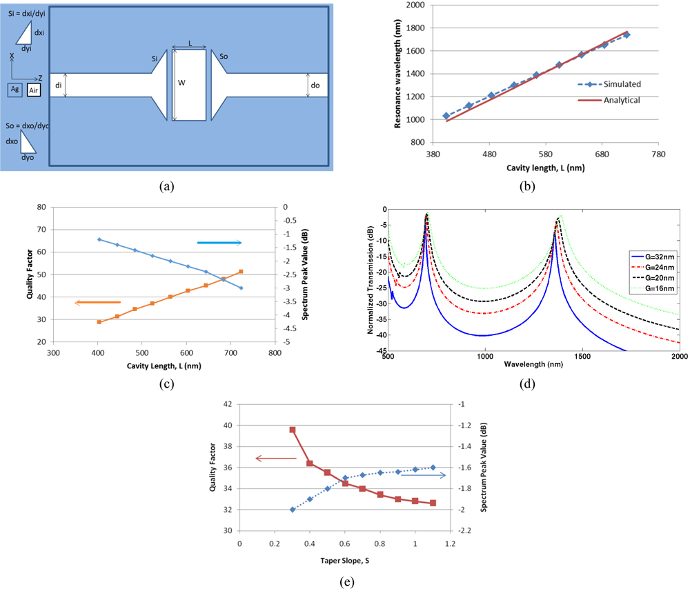
It can be seen from the results that as far as the cavity is wider than the waveguide, the wave does not monotonically transmit to the cavity and part of it is reflected and blocked. One way to compensate the mismatch is the novel structure presented in Fig. 2(a), in which the cavity input and output waveguides are tapered. Impacts of each parameter on the transmission spectra are illustrated in graphs of Fig. 3 and some numerical data including
[TABLE 3.] Simulated specifications of the single cavity NBPF with tapered waveguides of FIG. 2

Simulated specifications of the single cavity NBPF with tapered waveguides of FIG. 2
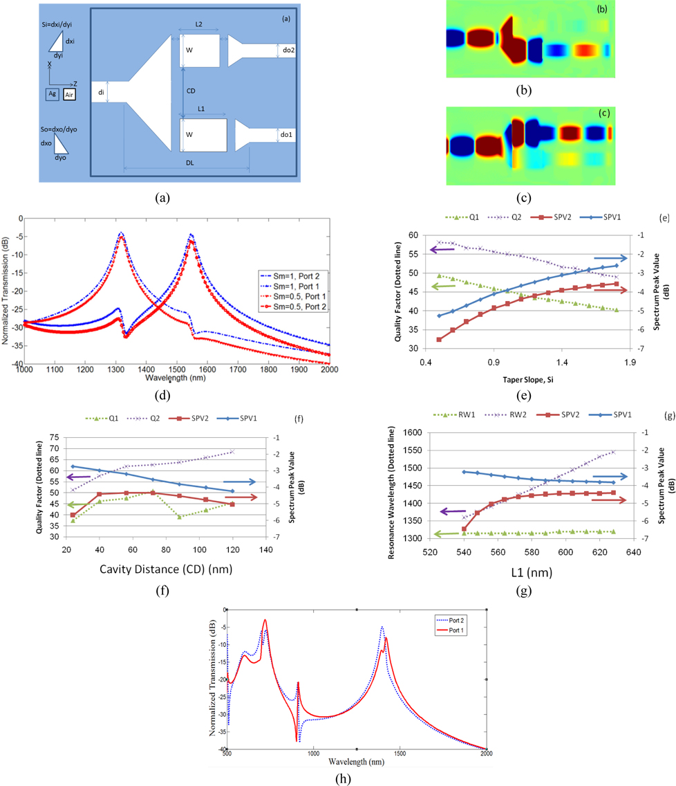
Another procedure for improving the specifications of the simple filter structure is to add another cavity along the waveguide, so that the filter could increase its selectivity. Figure 4(a) illustrates the proposed double cavity NBPF structure. It is important that the size of the metal between the two cavities, Gb, has to be thicker than a specific value, because if it is thin, the transmission spectrum shows two near-resonance wavelengths, which is the effect of coupling between the two cavities. The two cavities should be exactly the same to guarantee the same resonance wavelength. Figure 4(b), indicates the impact of the variation of the cavities’ length, L, on the transmission spectra. It can be noticed that as the length is increased, the quality factor and the resonance wavelength increase. The quality factor is improved, but the spectrum peak value is too low and the structure does not give desirable frequency response. In other words, when another cavity is added, although the selectivity is increased, the spectrum peak value is seriously decreased. To compensate again, we taper input and output waveguides of the new double cavity NBPF, as shown in Fig. 5(a). The impact of the variations of the cavities’ length and slope of the tapers on the transmission spectra are demonstrated in Fig. 5. Figures 5(b-c), show the linear relation of the resonance wavelength to L, for this structure, which resembles the analytical results with a good approximation, and it seems that adding another cavity does not noticeably change the empirical relation on resonance wavelengths of the cavities. Figure 5(d), similarly to the tapered single cavity filter, shows an approximate linear relation of spectrum peak value and quality factor to L. Table 4 gives the quantitative data on the effect of cavity length on the quality factor, resonance wavelength and spectrum peak value. In Fig. 5(e), the effect of variation of taper slopes (Si=So=S) on the quality factor and spectrum peak value is depicted.
[TABLE 4.] Simulated specifications of double cavity NBPF with tapered waveguides

Simulated specifications of double cavity NBPF with tapered waveguides
One of the specifications of a band-pass filter is its attenuation range (Astop), which shows the ability of the filter for damping the non-resonance wavelengths. It is shown in Fig. 5(f) as Astop. A good characteristic of the structure is its high attenuation range (approximately 40 dB), which can seriously damp the undesired wavelengths.
Four different structures’ spectra are compared in Fig. 6. There are significant improvements in the tapered NBPF structures. In the tapered single cavity structure, with the same loss in the transmission spectrum, the quality factor is improved and in the tapered double cavity NBPF, with the cost of minor decreases in spectrum peak value, the attenuation range significantly increases.
3.2. Ultra-compact Plasmonic Power Splitter
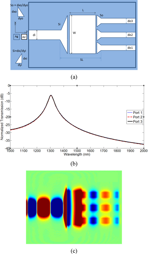
An ultra-compact splitter structure is presented based on the novel proposed single cavity NBPF structure, as shown in Fig. 7(a). The numerical result of the designed power splitter for the wavelength of 1310nm is depicted in Fig. 7(b). In Fig. 7(c), the impacts of the input taper slope, Si, on power splitter transmission are demonstrated. Increasing the taper slope could result in transmission with lower loss, but decreasing the quality factor and it also make the fabrication process more difficult, so there should be a trade-off between these parameters. The structures for plasmonic triple-wavelength and quartet-wavelength and the results of simulations to show the power splitting performance of the proposed devices are illustrated in Figs. 8 and 9, respectively. The output ports’ widths, do, can be designed to be narrower; so that more port power splitters can easily be achieved. The effective parameters for design of the structures are given in the figures’ captions. Power splitting with different ratios is also achievable by changing the distance of the output port from the cavity.
3.3. Ultra-compact Plasmonic Demultiplexer
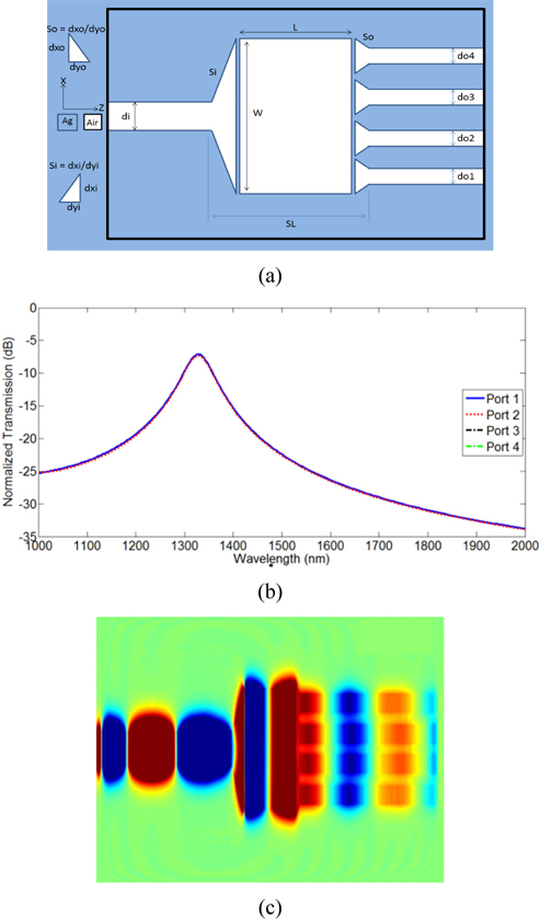
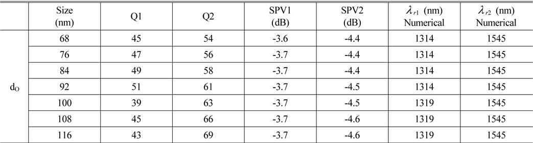
Based on the investigated structures, a novel demultiplexer system is presented in Fig. 10(a). The lengths of the cavities are adjusted so that the resonance wavelengths are 1310 nm and 1550 nm. Design parameters are given in the figure caption. Magnetic field distributions for two wavelengths are also demonstrated in Figs. 10(b) and (c) to show the demultiplexing performance of the device. The impacts of the input taper slope, Si, on the transmission spectrum are shown in Figs. 10(d-e). Steeper slopes cause better transmission with lower loss, but decrease the quality factor. Also, it would make the fabrication more difficult, so there should be a tradeoff. CD is the distance between the cavities, and it should be higher than a certain value to prevent coupling between cavities which would deteriorate the demultiplexing performance. The effect of CD on quality factor and spectrum peak value is investigated in Fig 10(f). We are interested in achieving a dense wavelength division demultiplexing. In Fig. 10(g), this possibility is tested, making one cavity length, L2, constant and slightly decreasing the other cavity length, L1, the resonance wavelength is collected and simultaneously the spectrum peak value is under supervision so that the loss is not a serious practical problem. In Fig. 10(h), we could successfully optimize and simulate a two-wavelength demultiplexer with resonance wavelengths of 1396 and 1417 nm, which is very desirable for dense plasmonic wavelength division multiplexing. Without taking footprints of the plasmonic filter, the demultiplexer length, DL is as small as 900 nm, which is a compact structure compared to other conventional demultiplexers, making it very desirable for photonic integrated circuits. In Tables 5 and 6, the effects of cavities’ width, W, and output ports’ width, do, are investigated. It is seen that changing do, does not change considerably the parameters of the achieved filter.
Effect of changing output ports’ width, do, on filter specifications of two-port demultiplexer. Assuming: di = 100 nm, L1 = 628 nm, L2 = 524 nm, W1 = W2 = 164 nm, G = 16 nm, Si = 0.5 and So = 1, CD=88 nm
Effect of cavities’ width, W=W1=W2, on filter specifications of two-port demultiplexer. Assuming: di = do = 100 nm, L1 = 628 nm, L2 = 524 nm, G = 16 nm, Si = 0.5 and So = 1, CD = 88 nm
The structure can be designed for triple-wavelength demultiplexing, as shown in Fig. 11. Again, resonance wavelengths are adjusted by variation of the cavities' lengths. We have designed the structure for the wavelengths of 1310, 1430 and 1550 nm. Magnetic field distributions for the 3 resonance wavelengths are illustrated in Figs. 11(c-e) to show the demultiplexing performance of the ultra-compact three channel demultiplexer. Owing to the flexibility for variation of the cavities’ lengths, other desired demultiplexing wavelengths, with even more channels which are distant enough, are achievable.
Two novel plasmonic slot cavity narrow band-pass filter (NBPF) structures have been proposed. The first one is a single cavity structure with tapered input and output waveguides, which increases the filter quality factor, and the second one consists of two successive cavities with the tapered waveguides, which increases the attenuation range of the filter. The devices are numerically analyzed and simulated by the two dimensional finite difference time domain (FDTD) method. Resonance wavelength and bandwidth can be adjusted by variation of the device parameters. Based on these filters, the novel plasmonic structures for two, three and four port splitter and two and three channel demultiplexers have been proposed, analyzed and simulated to demonstrate their performances. Different designs for power splitting and demultiplexing are achievable by adjusting the cavities' parameters with total length of less than 900 nm. Also, power splitters with different power ratios can be designed by varying the distance of the ports from the resonance cavities. Our results imply potential applications of the proposed structures in the nanoscale photonic integrated circuits on the flat metallic surfaces.


![Parameters of the Drude-Lorentz model for silver [25]](http://oak.go.kr/repository/journal/13401/E1OSAB_2014_v18n3_261_t001.jpg)