This paper presents the simulation and design of an all-optical subtractor using a quantum-dot semiconductor optical amplifier Mach-Zehnder interferometer (QD-SOA MZI) structure consisting of two cascaded switches, the first of which produces the differential bit. Then the second switch produces the borrow bit by using the output of the first switch and the subtrahend data stream. Simulation results were obtained by solving the rate equations of the QD-SOA. The effects of QD-SOA length, peak power and current density have been investigated. The designed gate can operate at speeds of over 250 Gb/s. The simulation results demonstrate a high extinction ratio and a clear and wide-opening eye diagram.
All-optical gates will be essential elements in future communications systems. All-optical processing has many applications, such as wavelength conversation, add-drop multiplexing, regeneration clock recovery, simple bit-pattern recognition, address recognition, signal processing, and packet synchronization [1-3]. Subtraction is one of the most important operations in Boolean functions and is used in binary subtraction, binary counting, arithmetic logic units, encryption, and decryption in security networks. Many designs for a single subtractor or subtractor with adder have been proposed by using a semiconductor optical amplifier (SOA) and periodically-poled lithium niobate (PPLN) waveguide [4], micro-ring resonator [5], exploiting four-wave mixing (FWM) in a SOA [6], a SOA based-Mach-Zehnder interferometer (MZI) [7], a three-state system [8], a terahertz optical asymmetric demultiplexer (TOAD) [9], a single-slot waveguide [10], two SOAs [11], implementing nonlinear material [12], and a nonlinear directional coupler [13]. SOA with quantum-dot active region is a promising candidate for ultrafast operations [14-15]. The high output power, low threshold current density, ultra-fast response behavior, good temperature stability, and low noise level of the quantum-dot SOA (QD-SOA) have been demonstrated, and it has been emphasized that these elements can be utilized as building blocks of alloptical systems [17-19]. In this paper, using two QD-SOA MZI, we design a subtractor that can operate and perform well at speeds of over 250 Gb/s.
II. REALIZATION OF ALL-OPTICAL SUBTRACTOR
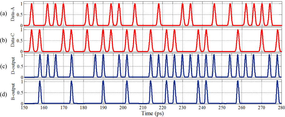
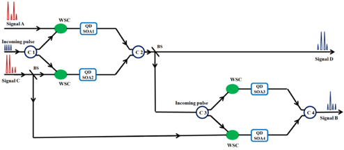
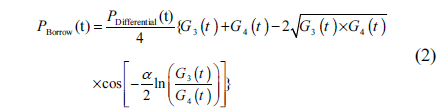
The subtractor is a combinational logic device that performs subtraction between two binary numbers. Its A and C inputs are for the minuend and subtrahend respectively. The differential and borrow outputs are D and B respectively. If A and C are equal then B=D=0, but if A=1 and C=0 then the outputs will be D=1, B=0. If A=0 and C=1 the outputs will be D=1 and B=1. Figure 1 shows the structure of our proposed subtractor. In the first MZI a differential bit is generated for which XOR operation has been done between A and C. Next the borrow bit is generated in the second MZI in which the differential bit acts as a probe signal. The theoretical results were verified by numerical simulation.
The output powers of the gate are expressed as,
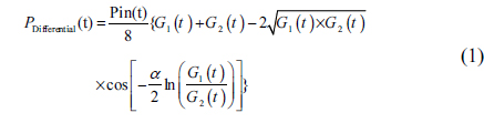
where Pin (t) denotes probe power that is a continuous wave pulse,


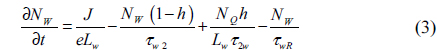
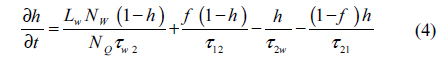
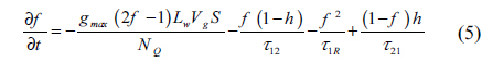
and the photon rate equation is
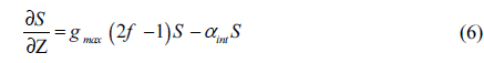
where z is the longitudinal direction along the QD-SOA length L, t is the local time, and
III. SIMULATION RESULTS AND DISCUSSION
In order to investigate the feasibility of the proposed design, we have applied the 4th-order Runge-Kutta method to solve equations (3-5) numerically and to calculate the gain coefficient. The input pulses are pseudo-random binary sequences at 250 Gb/s whose profile is Gaussian, that is where
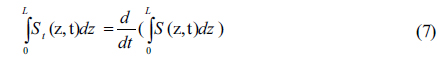
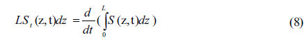
and by integrating along the z variable in equation (7) we have

The next integration along the t variable in equation (8) gives
where (

where
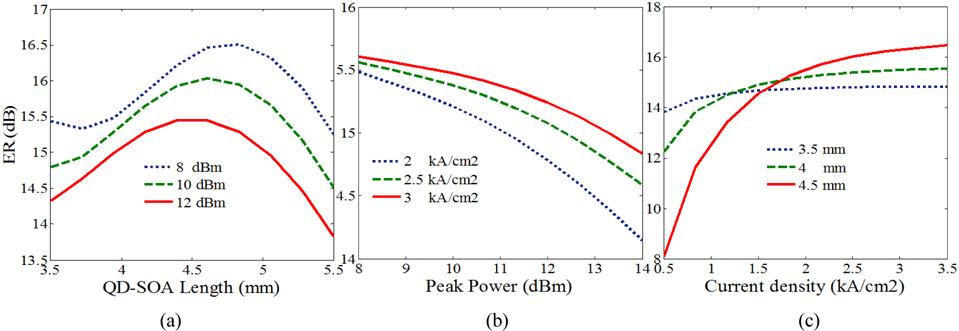
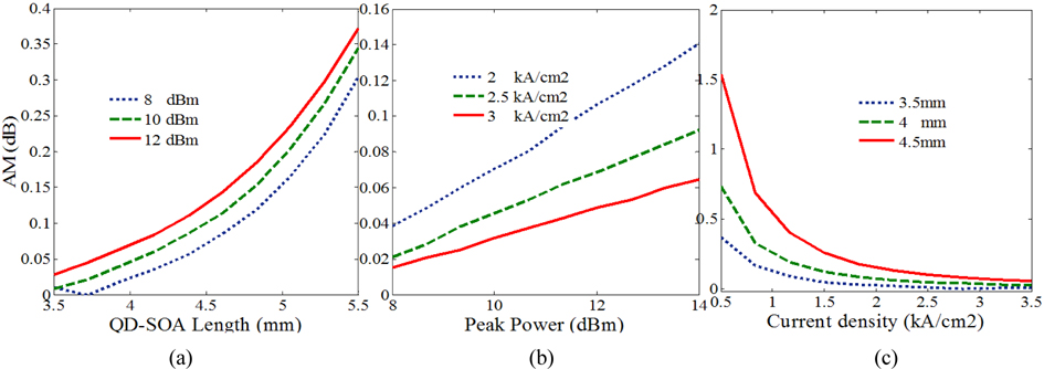
where and are the minimum and maximum values of the peak power of “1” and “0”, respectively [23]. In order to distinguish 1 unambiguously from 0 the ER must be over 10 dB [23]. Figure 2(a) depicts the ER variation versus QD-SOA length for three different peak power values of input data signals, where the other parameters are kept fixed. It is observed in the curves that for 4 <
The ratio between maximum and minimum peak power for signals corresponding to “1” is defined as
where and is the maximum peak power of “1” and “1” respectively [24]. The lower the AM, the more uniform is the level of the “1” outputs, and the smaller is the related pattern effect. Figure 3(a) illustrates the effect of QD-SOA length on the AM for three different peak powers of input data signals. For
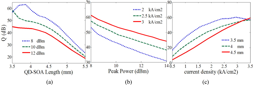
The quality factor is defined as
where
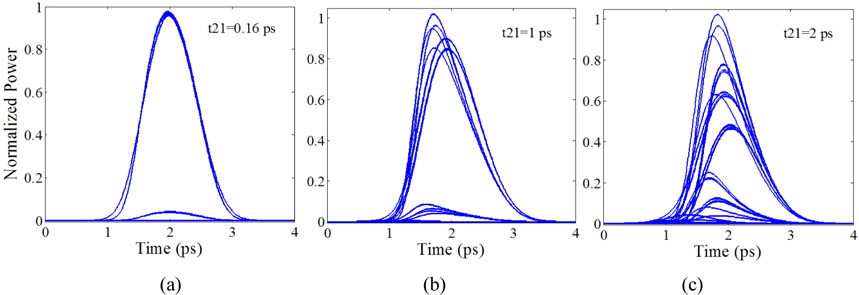
A pseudo-eye diagram is one of the best standards for assessing the output signals. A clear and open eye diagram is desired. Figure 5 illustrates the effect of electron relaxation time from ES to GS on PED. A slow transition of the electron between ES and WL results in a slower cross gain modulation. Thus speed is limited by the relaxation time from the wetting layer to the quantum-dot state.
The relative eye opening is defined as

where and are the minimum and maximum powers for ones and zeros respectively [10]. In this design the related eye opening is over 90%. Table 1 shows the relative eye opening for three QD-SOA lengths and three electron relaxation times from ES to GS. The other parameters are kept fixed.
[TABLE 1.] Variations of relative eye opening with L and ?21

Variations of relative eye opening with L and ?21
According to Figs. 2-5 and our discussions so far, QDSOAs with lengths smaller than 4.5 mm, show desirable responses but smaller lengths decrease unsaturated gain. Table 2 shows gain values for five different QD-SOA lengths. It was found that with current density of more than 2.5
[TABLE 2.] Variation of QD-SOA gain with length

Variation of QD-SOA gain with length
According to the above mentioned explanations and using the combination of input parameters
Table 3 illustrates the output parameters of the proposed structure, compared to those of similar recent structures. The last column shows the parameters of our designed structure, which demonstrates its better performance, due to our choice of optimal parameters for the structure, and use of the transmitting ports in both MZIs.
[TABLE 3.] The comparison of parameters of the proposed optical gate with those of other papers
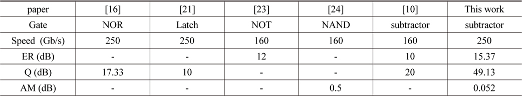
The comparison of parameters of the proposed optical gate with those of other papers
The main reason for the faster response of a QD-SOA compared to a bulk SOA is the presence of the wetting layer. The wetting layer serves as a carrier reservoir: Carriers depleted by the injected optical pulse in the QD ground state are replaced from the wetting layer by fast carrier transfer. At a higher injected current density there are more carriers in the wetting layer, resulting in a better performance. Thus the speed of optical logic gates is limited by the carrier recovery time in the device. Careful adjustment of the peak power of the modulated signal and QD-SOA bias current is necessary for error-free performance at high data rates and for avoiding overlap in response.
The effects of the most important parameters on the performance of the proposed gate are investigated using a model of three coupled equations for a QD-SOA into which a Gaussian pulse with rate 250 Gb/s has been inserted. The results show that output signals have high ER and Q and low AM, and that the gate can operate well at speeds of over 250 Gb/s. In both MZIs we used the transmitting port. The reflecting port can also be used to extend the device in generating other logic gates.