This paper presents an advanced patterned vertical aligned nematic liquid crystal (APVA) mode as a way of improving the transmittance of the conventional patterned, vertically-aligned nematic liquid crystal (PVA) mode. The APVA was characterized by multi-electrodes, which play an important role in generating a horizontal electric field that prevents LC disclination in the vicinity of the middle region of electrodes between top and bottom slits in PVA mode. The proposed APVA mode focused on improving dramatically the transmittance with excellent image quality. In the simulation, the APVA mode improved the transmittance by more than 22%, compared to the conventional VA modes. Therefore, it is useful to upgrade the LCD display quality.
The bright levels of liquid crystal displays (LCDs) are controlled by electrically modulating the optical anisotropy of LCs, determining the polarization state of light. Improved controllability of the electro-optical characteristics in LCD technologies, such as contrast ratio, response time and viewing angle, has enabled TFT-LCDs to expand rapidly in the display market. Recently, high efficiency LCDs with high aperture ratios have become more interesting because they can achieve more vivid images and reduce the power consumption, thus saving energy. Several types of LCD modes [1-21] that are determined by the initial LC configuration and electrode structure, have been proposed, including twisted nematic (TN), in-plane switching (IPS), and vertically aligned (VA) modes.
The IPS mode has excellent viewing angle characteristics without the need for an optical compensation film because of the similar effective retardation of the LC layer at the off-axis to that of the on-axis. IPS mode also displays uniform gray levels and colors but it has relatively low transmittance compared to the TN mode because LCs are aligned almost vertically on the electrode due to the direction of the electric field.
As a competitor of IPS mode, vertical aligned (VA) nematic modes with multi-domain LC structures have been attractive in LC displays because of their high contrast ratios. The patterned VA (PVA) mode is a representative VA mode that is characterized by its chevron-shaped electrode to induce four domain-LC-structures to produce practical wide viewing angles with adopting compensation films and very high contrast ratios resulting from its excellent dark state. On the other hand, it has also demerits, such as slow rising speed and low transmittance due to disclination formation of LC molecules driven from the direction matching between the electric field and initial LC alignment in the vicinity of the middle region between the top and bottom slits, as shown in Fig. 1. To overcome these problems, namely to eliminate the disclination and improve the rising speed, Kim’s
In a more desirable case, this paper presented vertical aligned nematic mode with the surface morphology [20]. The LCD should show uniform electro-optic characteristics at all viewing angle directions, which can be achieved using a LC cell with an azimuthally omnidirectional LC direction distribution, which is also known as a real multidomain structure. Therefore, it is essential to design a new type of electrode to create an advanced LCD to drive this type of wide viewing directional capability. On the other hand, this mode has a difficult fabrication process. This paper presents a new LCD display mode, field-controlled vertical alignment (FVA) nematic mode, which is characterized by additional stripe type common electrodes that play important roles in generating a horizontal electric field that prevents LC disclination in the vicinity of the middle region of the electrode to improve the transmittance in PVA mode [21]. FVA mode, however, has a limitation for improving the transmittance because the horizontal electric field cannot be increased greatly, which affects the initial black state.
In this paper, as an upgraded vertical aligned LCD mode, this paper presents an advanced patterned vertical aligned nematic liquid crystal (APVA) mode to obtain high transmittance and rapid response time. This mode is characterized by multi-electrodes that play important roles in generating a horizontal electric field that prevents LC disclination in the vicinity of the middle region of the electrodes between top and bottom slits in PVA mode. The proposed APVA mode improves the transmittance dramatically with excellent image quality.
II. SIMULATION WITH ELECTRODE CONFIGURATION IN CELL
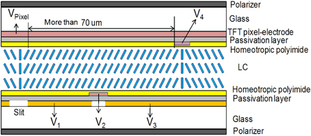
Figure 2 shows a schematic diagram of the unit LC cell structure of the proposed LCD mode. For the top substrate, the overall indium-tin-oxide (ITO), as a TFT-pixel electrode, was coated by sputtering on the glass substrate. SiO2 was deposited on an ITO electrode to prevent an electric short between the overall ITO electrode and pattern ITO electrode (V4). For the bottom substrate, the two ITO electrodes with fixed different voltages (V1 and V3) were patterned on glass. SiO2 was deposited on ITO electrodes to prevent an electric short between the two ITO electrodes and pattern the ITO electrode (V2) on it. The vertical LC alignment material was also spin-coated on it and baked on a hot plate under the same conditions as the top substrate for polymerization. The LC material used for the simulation was MLC-6610 (Merck), which has Δn = 0.09 and Δε= -3.1. The cell thickness was 3.5 μm. The simulation was performed using a commercial LCD simulator, Techwiz 3D-LCD. As the driving schematic, when a positive voltage is applied to the pixel electrode in frame order, V1 should be a positive voltage approximately near 1.5 V because if the voltage is more than 1.5 V, it might move the LCs in the initial state and might affect the minimum dark state. V2 is 0 V as the base voltage, and V3 and V4 should be negative voltages at approximately -1.5 V. When a negative voltage is applied to the pixel electrode in frame order, V1 should be a negative voltage of approximately -1.5 V, V2 is 0 V as a base voltage, and V3 and V4 should be positive voltages of approximately 1.5 V. Here, because the horizontal electric fields by the voltage format of V1= 1.5 V, V2= 0 V, and V3 = -1.5 V (or V1 = -1.5 V, V2 = 0 V, and V3 = 1.5 V) are in one direction (right or left), the lying of LCs on the V1, V2 and V3 electrodes are in the same direction. Consequently, this electrode structure and driving method of each electrode can increase the domain size of LCs in a pixel by more than double compared to that of the conventional PVA, whose domain size in a pixel is approximately 30 μm, as shown in Fig. 2. As a result, it is expected that the proposed PVA mode will produce very high transmittance.
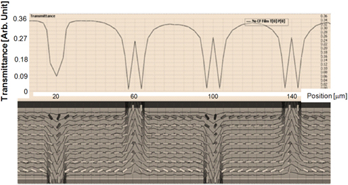
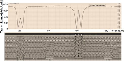
Figure 3 shows the transmittance according to the position of the pixel when 8 V is applied to the pixel electrode of the conventional PVA mode with the electrode structures of 10 μm (slit width): 30 μm (the distance between the top and the bottom slits). As shown in Fig. 3, the transmittance of the PVA mode is not high because the transmittance always decreases at each slit region. In addition, the vertical electric field of the center region between the top and bottom slits confuses the vertically aligned LCs on the decision of the azimuthally lying direction, so- called disclination formation of LCs. Therefore, the response speed of PVA mode slows. In addition, expansion of the distance between slits was performed to increase the transmittance. On the other hand, its expansion aggravates the disclination formation of the LCs to the wider region and the response speed is slower.
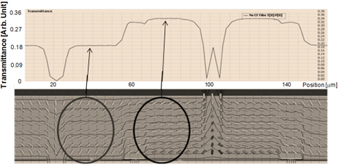
As shown in Fig. 4, the APVA mode has higher transmittance because an LC tilt of the same direction in the wider region including the central slit region is produced. As a result, the proposed APVA mode can also lead to a faster response speed.
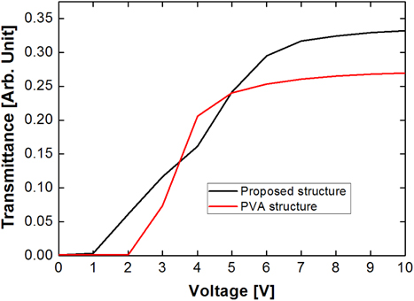
Figure 5 compares the voltage-transmittance curves of the PVA mode with the electrode structures of 10 μm : 30 μm and the APVA mode with electrode structures of 10 μm (the width of the stripe type electrode): 30 μm (the distance between the top and the bottom stripe type electrodes). As expected, the transmittance of the APVA mode is 22.7% higher than that of the PVA mode: the maximum transmittances in the typical PVA mode and APVA mode are 0.269 and 0.33, respectively.
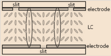
As an additional merit of the APVA mode, Fig. 6 shows that the APVA mode can exhibit 8 domains at the grey level at 5 V. This is unlike the PVA mode, which exhibits 4 domains. The 4 domain structure at the PVA is inferior to IPS mode in terms of the color shift. The PVA mode requires 8 domains with compensation films to show excellent color characteristics at the side view. To achieve 8 domains in PVA mode, it should use a two TFT structure, so called SPVA (Super PVA), showing a lower transmittance due to two TFTs.
On the other hand, the proposed APVA mode shows 8 domains without an additional TFT. This was attributed to the different electric field at the right and left regions of the slit. The LCs were laid down first at the region with a relatively strong electric field shown in the black circle in Fig. 6, whereas the LCs were tilted slightly at the region with a relatively weak electric field shown in the red circle mark of Fig. 6. To obtain better color characteristics, the ratio of the right and left regions of the slit and the voltages of each electrode (V1, V2, V3, and V4) were designed properly.
This paper proposed an advanced patterned vertical aligned nematic liquid crystal (APVA) mode characterized by multi-electrode switching the polarity voltage, which plays an important role in generating a horizontal electric field that prevents LC disclination in the vicinity of the middle region of the electrodes shown in the patterned vertically aligned nematic liquid crystal mode (PVA mode). The proposed APVA mode showed dramatically improved transmittance with excellent image quality. In a quantitative evaluation, the APVA mode improved the transmittance by 22%, compared to the conventional VA modes. Consequently, this mode will be useful for upgrading the LCD display quality.