검색 전체 메뉴
PDF
맨 위로
OA 학술지
Lasing of Coupled Guided Modes in Modified Hollow Hexagonal Semiconductor Cavities
  • 비영리 CC BY-NC
  • 비영리 CC BY-NC
ABSTRACT
Lasing of Coupled Guided Modes in Modified Hollow Hexagonal Semiconductor Cavities
KEYWORD
Coupled guided modes , Hollow hexagon , Microcavity laser
  • I. INTRODUCTION

    Polygonal microcavities such as squares and hexagons, and polygonal ring cavities such as square ring cavities have attracted a great deal of interest due to the existence of whispering gallery (WG)-like modes, similar to WG modes in disk-type cavities, originating from the total internal reflection (TIR) of light at the boundaries [1-7]. Microcavities based on WG or WG-like modes are considered to be potential building blocks in photonic integrated circuits for optical filtering, switching, and microlasers [8-12]. Because the aforementioned cavities have flat sides, they present strong advantages, such as a long interaction length during coupling with external flat waveguides [13, 14].

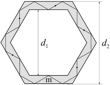
    Recently, a different type of WG-like modes called “guided modes” have been reported in hollow polygonal (square or hexagonal) geometries, wherein TIR occurs not only at the outer boundaries but also at the inner boundaries [15-17]. Figure 1 shows the previous hollow hexagonal cavity (outer size d2, inner size d1, and refractive index m) and the ray trajectory corresponding to the guided modes [17].

    If the inner size d1 is quite a bit smaller than d2, WG-like modes are expected to bounce 6 times only at the outer boundaries, with an incident angle of 60°. If d1 is slightly smaller than d2, the possible modes are no longer the 6-bounce ones. Under the condition of 3d2/4 <d1 <6d2/7, 18-bounce WG-like modes called “guided modes” are selected as the resonance modes, as shown in Fig. 1 [17]. The optical path length L during one round trip, is calculated as [17]

    where l is the round-trip length of the guided modes. The resonance wavelength λ q can be approximately determined from a ray-optics picture as

    where q is an integer, and Ψ (60°) is the phase change during total internal reflection at the outer or inner boundaries. Equation (2) has a limitation in calculating the exact λq because there is a large number of bounces during one round trip, where each bouncing produces the Goos-Hänchen effect [18]. The mode spacing Δλ (=λq−1λq) between two adjacent modes can be derived from Eq. (2).

    One advantage of the guided modes is the tunable property of the resonance structure achieved by adjusting inner size d1 for a common outer size d2. Thus the roundtrip length l or the mode spacing Δλ can be also adjusted by changing the inner size d1. Therefore, it is expected that a hollow polygonal cavity can be a tunable building block for photonic integrated circuits. By standardizing the outer size, multiple cavities with different mode structures can be simultaneously coupled to a straight waveguide or pairs of straight waveguides, which permits additional functionality for the resonance structure of the coupled cavities.

    However, there is a limitation for the guided modes in a hollow polygonal cavity in an actual structure: The adjustable range δλ in Δλ is very small because the guided modes exist in a very narrow range of inner size d1 for a fixed outer size d2. In a rough calculation, the adjustable range δλ in a hollow hexagonal cavity is limited to only ~5% of Δλ (δλλ ~ 0.05). Hence, the guided modes in a hollow polygonal cavity are limited to certain fine-tuning applications.

    II. PROPOSED COUPLED GUIDED MODES

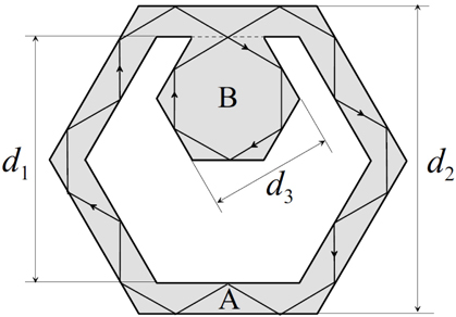
    In this study, we propose a modified guided mode (denoted as a “coupled guided mode”) with a very large adjustable range in a modified hollow polygonal cavity, wherein a polygon is attached internally, so that the guided modes extend to the entire cavity. An example is shown in Fig. 2, in which a hexagon B (size d3) is attached at the center of an inner side of external hollow hexagonal cavity A (outer size d2, inner size d1).

    The guided modes in Fig. 1 extend to internal hexagon B, as depicted in Fig. 2. It is notable that there is no loss experienced by the light passing through the joint region, and this scheme is not limited in the wavelength of light. The elongation of the round-trip length by simply attaching the additional cavity is difficult to realize with other cavity geometries, such as MMI-coupled racetrack geometries [19]. If two racetrack cavities are coupled by MMI with a power coupling coefficient of ≅1, light can jump from one cavity to the other at the MMI coupler, resulting in the extension of the cavity modes, but the wavelengths satisfying ≅1 are limited to a small range because depends on the wavelength of the light. Moreover, there is the insertion loss of the MMI coupler. Thus the proposed scheme cannot be directly applied to racetrack geometries. The optical path length L corresponding to the resultant modes increases from Eq. (1) as

    Because d3 can be varied over a wide range (from 0 to about d1) for a given hollow hexagonal cavity A, a large change in the mode spacing Δλ is expected for the coupled guided modes. The calculated adjustable range δλ in Δλ can amount to about 60% of Δλ , which is much larger than the aforementioned 5%, just by controlling d3 for a given external cavity. Therefore, the proposed cavity could be a versatile building block with large scalability in the resonance structure. In applications for switching, fine tuning of resonance modes might be also required by locally changing the refractive index of the cavity via current or heat. The modified cavity in Fig. 2 is ideal for this application because the fine-tuning functionality can be realized specifically on the internal hexagon B. In this study, we demonstrated the lasing of the proposed coupled guided modes in a modified hollow hexagonal semiconductor cavity and investigated the dependence of the lasing spectrum on the internal size.

    III. EXPERIMENTS

    The experimental setup and epistructure used for the semiconductor cavities were similar to those in our previous studies [16, 17]. InGaAsP/InGaAs multiple quantum wells (MQWs, λ g≅1.55 μm) surrounded by two confinement layers were used for the laser gain medium. The total thickness of the epistructure formed on an InP substrate was about 3 μm. Various cavities were lithographically patterned and fabricated by inductively coupled plasma (ICP) etching, unlike the previous RIE (reactive ion etching) process. The total etching depth of about 4 μm was sufficient for lasing. A pulsed Nd:YVO4 laser (wavelength 1.06 μm, repetition rate 10 kHz, pulse width 300 ns) was loosely focused on a cavity to optically pump the MQWs. The illuminated cavity was monitored using a CCD camera attached to a high-resolution microscope. A tapered fiber approached a corner of the illuminated cavity to collect the lasing signal; the other end of the tapered fiber was connected to an optical spectrum analyzer for measurement of the lasing spectrum. We confirmed that the measured signal is due to lasing by observing the threshold behavior of the spectral peak intensity. The threshold laser pulse energy was about 2 μJ when the illuminated spot size of the pulsed pump beam on the wafer was about 500 μm, which corresponded to a peak pump intensity of ~3 kW/cm2.

    IV. RESULTS & DISCUSSIONS

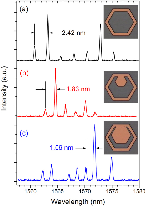
    Figure 3 shows typical lasing spectra, measured at ~3 times the threshold pump level, for hollow hexagonal external cavities (d2 = 80 μm, d1 = 64 μm) with various sizes d3 of the internal hexagon. It is notable that parameters d2 and d1 satisfy the condition for guided modes in Fig. 1. For the case of d3 = 0 (no internal hexagon), the lasing peaks appeared around 1570 nm with a mode spacing Δλ of about 2.42 nm, as shown in Fig. 3(a). The lasing modes should be the 18-bounce guided modes of Fig. 1. For the cases of d3 = 30 μm and 50 μm the mode spacing was reduced to about 1.83 nm and 1.56 nm respectively, as shown in Fig. 3. (b) and (c). The reduction of the mode spacing implied that the optical path length increases with the size of the internal hexagon. Therefore, the lasing modes should not be the 18-bounce guided modes of Fig. 1 but could be the 22-bounce coupled guided modes shown in Fig. 2.

    The mode spacing Δλ of the resonance modes in a semiconductor laser can be expressed as [16, 17]

    where the group index M(λ ) accounts for the dispersion in the semiconductor material and is weakly dependent on λ .

    Because all the center wavelengths of the lasing spectra were similarly observed around 1565 nm in Fig. 3, the group index M(λ ) can be considered constant. Thus the mode spacing in Eq. (4) should be inversely proportional to the round-trip length l of the resonance modes. If the lasing peaks in Fig. 3(b) are the proposed coupled guided modes, the mode-spacing ratio (2.42 nm/1.83 nm ≅1.32) between Fig. 3(a) and (b) should be equal to the inverse ratio of the corresponding l’s. The calculated inverse ratio of l (378 μm/288 μm ≅1.31), using Eq. (4) and (3), is essentially the same as the measured mode-spacing ratio of 1.32. Therefore, the lasing modes should be the coupled guided modes as conjectured.

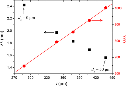
    Figure 4 summarizes the mode spacing Δλ measured at λ ~ 1565 nm from the common external cavities (d2 = 80 μm, d1 = 64 μm) with different d3 (0, 20, 30, 40, and 50 μm). In Fig. 4, the dependence of λλ on the round-trip length l in Eq. (3) is also shown. λλ showed a linear dependence on l with a slope of 2.349 (μm−1). Therefore, M(λ ) in Eq. (4) was derived as 2.349 (μm−1) 1.565 μm ≅ 3.67. This is slightly larger than the previously reported value, due to the different epistructure and center wavelengths of the lasing [16]. The linear relation between λλ and l in Fig. 4 strongly confirms the lasing of the coupled guided modes in Fig. 2.

    In Fig. 4, the mode spacing Δλ gradually decreased as d3 increased. It is notable that Δλ varied over a wide range, i.e. the adjustable range δ λ was very large. For example, Δλ changed about 55% from the case of d3= 0 to that of d3 = 50 μm (i.e. 2.42 nm/1.56 nm ~ 1.55). Therefore, the coupled guided modes showed a widely adjustable resonance structure, as proposed.

    To verify whether coupled guided modes exist for other sizes of the external cavity, various other external cavities were also designed and fabricated. Figure 5 shows typical lasing spectra with different common sizes (d2 = 100 μm, d1= 80 μm). As d3 of the internal hexagon increases from 0 to 20 μm to 60 μm, the mode spacing Δλ of the lasing peaks decreased from about 1.95 nm (Fig. 5(a)) to 1.7 nm (Fig. 5(b)) and 1.26 nm (Fig. 5(c)) respectively. The reduction of the mode spacing should be also interpreted as the lasing of the coupled guided modes in Fig. 2, as observed in Fig. 3.

    The 18-bounce guided mode lasing in Fig. 5(a) appeared at ~ 1573 nm. The lasing peaks in Fig. 5(a) seem to be irregular as the mode spacing between several peaks on the left was not the same. This irregular feature should be attributed to the simultaneous lasing of coupled guided modes with two different polarizations (TE and TM). It is notable that the center wavelength of the lasing in Fig. 5(b) appeared at ~ 1563 nm, which is quite a bit shorter than that in Fig. 5(a). The center wavelength tends to appear in a lower absorption region (longer wavelength) as the total cavity loss decreases, as explained previously [17]. Thus the blue-shift of the center wavelength implies that the total cavity loss of the resonance modes increased. One reason might be the larger bouncing number of the 22-bounce coupled guided modes than the 18-bounce guided modes. More frequent bouncing during one round trip will yield a much greater total loss because scattering loss in the TIR process comes from the roughness of the etched surface. However, this seems unlikely because an apparent blue-shift was not observed in Fig. 3 for the same increase in bouncing number.

    The other plausible origin is due to the smaller side length of the internal hexagon. Due to the Goos-Hänchen effect, a ray-propagation distance exists for the TIR process at the flat boundary [18]. Thus an evanescent wave exists along the flat side within a finite length of propagation. The evanescent wave could leak from the boundary corner. As the flat side length of the internal hexagon becomes smaller, more evanescent leakage loss from the corner is expected. Therefore, the quality factor Q of the coupled guided modes will be rapidly spoiled when d3 becomes smaller than a certain value. The Q-spoiling in Fig. 5(b) can be attributed dominantly to this evanescent leakage loss. Thus too small d3 should be avoided for high-Q coupled guided modes in real applications.

    V. CONCLUSION

    In conclusion, resonance modes called coupled guided modes were proposed in a hollow polygonal cavity in which an additional polygon is attached internally. In the case of a hollow hexagonal cavity, 18-bounce guided modes were modified to 22-bounce coupled guided modes using an internal hexagon to extend the round-trip length. The proposed coupled guided modes were demonstrated by investigating the lasing spectra in various semiconductor cavities. The adjustable range in the mode spacing became about 10 times larger than for the previous guided modes, which will be beneficial for tunable photonic building blocks with common outer size. This scheme can be expanded to different polygonal shapes, such as square and octagonal geometries.

참고문헌
  • 1. Poon A. W., Courvoisier F., Chang R. K. 2001 Multimode resonances in square-shaped optical microcavities [Opt. Lett.] Vol.26 P.632-634 google
  • 2. Huang Y. Z., Che K. J., Yang Y. D., Wang S. J., Du Y., Fan Z. C. 2008 Directional emission InP/GaInAsP squareresonator microlasers [Opt. Lett.] Vol.33 P.2170-2172 google
  • 3. Ma N., Li C., Poon A. W. 2004 Laterally coupled hexagonal micropillar resonator add-drop filters in silicon nitride [IEEE Photon. Technol. Lett.] Vol.16 P.2487-2489 google
  • 4. Gargas D. J., Moore M. C., Ni A., Chang S. W., Zhang Z., Chuang S. L., Yang P. 2010 Whispering gallery mode lasing from zinc oxide hexagonal nanodisks [ACS Nano] Vol.4 P.3270-3276 google
  • 5. Hyun K. S., Moon H. J. 2010 Resonant characteristics of multimode interferometer coupled square ring semiconductor resonators [Opt. Express] Vol.18 P.6382-6389 google
  • 6. Hyun K. S., Lee T., Moon H. J. 2012 Single mode lasing in InGaAsP/InP semiconductor coupled square ring cavities [J. Opt. Soc. Korea] Vol.16 P.157-161 google
  • 7. Armani D. K., Kippenberg T. J., Spillane S. M., Vahala K. J. 2003 Ultra-high-Q toroid microcavity on a chip [Nature] Vol.421 P.925-928 google
  • 8. Savchenkov A. A., Ilchenko V. S., Matsko A. B., Maleki L. 2005 High-order tunable filters based on a chain of coupled crystalline whispering gallery-mode resonators [IEEE Photon. Technol. Lett.] Vol.17 P.136-138 google
  • 9. Cai M., Painter O., Vahala K. J. 2000 Observation of critical coupling in a fiber taper to a silica-microsphere whispering-gallery mode system [Phys. Rev. Lett.] Vol.85 P.74-77 google
  • 10. Van V., Ibrahim T. A., Ritter K., Absil P. P., Johnson F. G., Grover R., Goldhar J., Ho P.-T. 2002 All-optical nonlinear switching in GaAs?AlGaAs microring resonators [IEEE Photon. Technol. Lett.] Vol.14 P.74-76 google
  • 11. Moon H. J., Chough Y. T., An K. 2000 Cylindrical microcavity laser based on the evanescent-wave-coupled gain [Phys. Rev. Lett.] Vol.85 P.3161-3164 google
  • 12. Spillane S. M., Kippenberg T. J., Vahala K. J. 2002 Ultralow-threshold Raman laser using a spherical dielectric microcavity [Nature] Vol.415 P.621-623 google
  • 13. Moon H. J., Hyun K. S. 2012 Bow-tie mode lasing in a grooved rectangular semiconductor microcavity [J. Opt. Soc. Korea] Vol.16 P.162-165 google
  • 14. Fong C. Y., Poon A. W. 2004 Planar corner-cut square microcavities: Ray optics and FDTD analysis [Opt. Express] Vol.12 P.4864-4874 google
  • 15. Moon H. J., Sun S. P., Lee J. H., An K. 2003 Guided mode lasing in a double-layered square microcavity [Appl. Phys. Lett.] Vol.83 P.2521-2523 google
  • 16. Moon H. J., Hyun K. S. 2007 Selective lasing of guided modes from hollow square semiconductor microcavties [Jpn. J. Appl. Phys.] Vol.46 P.L274-L276 google
  • 17. Moon H. J. 2009 Enhanced lasing characteristics of guided modes in an epistructured hollow hexagonal cavity [Jpn. J. Appl. Phys.] Vol.48 P.030205 google
  • 18. Saleh B. E. A., Teich M. C. 1991 Fundamentals of Photonics, Chapter 7 google
  • 19. Rabus D. G., Hamacher M. 2001 MMI-coupled ring resonators in GaInAsP?InP [IEEE Photon. Technol. Lett.] Vol.13 P.812-814 google
OAK XML 통계
이미지 / 테이블
  • [ Fig. 1. ]  Ray trajectory for 18-bounce guided modes in a hollow hexagonal cavity (outer size d2, inner size d1, and refractive index m) with an incident angle of 60°.
    Ray trajectory for 18-bounce guided modes in a hollow hexagonal cavity (outer size d2, inner size d1, and refractive index m) with an incident angle of 60°.
  • [ FIG. 2. ]  Proposed modified hollow hexagonal external cavity, in which a hexagon (size d3) is attached internally. The corresponding ray trajectory for 22-bounce coupled guided modes is also shown.
    Proposed modified hollow hexagonal external cavity, in which a hexagon (size d3) is attached internally. The corresponding ray trajectory for 22-bounce coupled guided modes is also shown.
  • [ FIG. 3. ]  Typical lasing spectra of modified hollow hexagonal semiconductor cavities (d2 = 80 μm, d1 = 64 μm) with internal hexagons of (a) d3 = 0, (b) d3 = 30 μm, (c) d3 = 50 μm. Microscopic images of the cavities are also shown.
    Typical lasing spectra of modified hollow hexagonal semiconductor cavities (d2 = 80 μm, d1 = 64 μm) with internal hexagons of (a) d3 = 0, (b) d3 = 30 μm, (c) d3 = 50 μm. Microscopic images of the cavities are also shown.
  • [ Fig. 4. ]  Dependence of measured mode spacing Δλ (black squares) and λ /Δλ (red circles) on the calculated round-trip length l for common external cavities (d2 = 80 μm, d1 = 64 μm) with various d3 (0, 20, 30, 40, 50 μm).
    Dependence of measured mode spacing Δλ (black squares) and λ /Δλ (red circles) on the calculated round-trip length l for common external cavities (d2 = 80 μm, d1 = 64 μm) with various d3 (0, 20, 30, 40, 50 μm).
  • [ FIG. 5. ]  Typical lasing spectra of modified hollow hexagonal semiconductor cavities (d2 = 100 μm, d1 = 80 μm) with internal hexagons of (a) d3 = 0, (b) d3 = 20 μm, (c) d3 = 60 μm.
    Typical lasing spectra of modified hollow hexagonal semiconductor cavities (d2 = 100 μm, d1 = 80 μm) with internal hexagons of (a) d3 = 0, (b) d3 = 20 μm, (c) d3 = 60 μm.
(우)06579 서울시 서초구 반포대로 201(반포동)
Tel. 02-537-6389 | Fax. 02-590-0571 | 문의 : oak2014@korea.kr
Copyright(c) National Library of Korea. All rights reserved.