Power amplifier (PA) is a key component in mobile handsets, but designing PA is still challenging because high efficiency as well as high linearity is demanded without any compromise for 3G/4G mobile standard applications. For this reason, high performance devices, such as GaAs HBT/HEMT, have mostly been employed for commercial PA fabrication. On the other hand, the CMOS PA has been widely researched to take advantage of its low cost and high integration capability. The weaknesses of the CMOS device/process (e.g., low breakdown voltage and no substrate via hole to the ground) have been overcome by using power combining techniques such as the stacked field-effect transistor (FET) and transformer-based differential cascode structures. Watt-level power amplification has thus been achieved in recent years [1-3]. However, the nonlinear characteristics of the CMOS device have prevented the CMOS PA from being used in actual 3G/4G handset PA applications where stringent linearity is required.
To enhance the linearity of a CMOS PA, several linearization techniques have been proposed. The use of a variable capacitor at the common-gate (CG) FET and envelope-reshaped gate bias technique effectively improved the PA linearity [2,3]. As explained in [4,5], one of the major nonlinearities of a CMOS device comes from the gatesource capacitance (
In this work, a highly linear and efficient watt-level CMOS PA is implemented using an integrated PMOS linearizer for low-band UMTS Tx applications. The problem described above is resolved by employing a PMOS linearizer with optimized AM-PM at the input of the driver-stage, thereby compensating the composite nonlinearity coming from the two amplifiers. In this paper, the detailed circuit design of the proposed linear PA is presented in Section II, followed by the fabrication and measurement results of the PA in Section III.
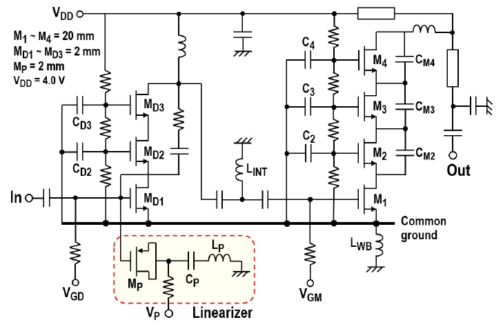
Fig. 1 shows a schematic of the proposed linear CMOS PA. It is based on a two-stage single-ended stacked-FET amplifier design [1], and is targeted to obtain an output power (
As described in [4,5], the nonlinear gate-source capacitance (

In this work,
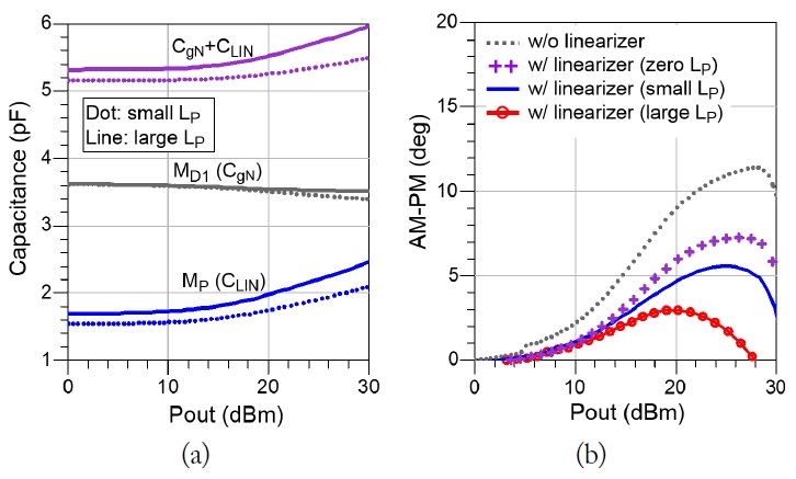
Fig. 3 shows the simulated capacitance at the gate of the driver-stage and resultant AM-PM of the composite PA. The composite input capacitance (
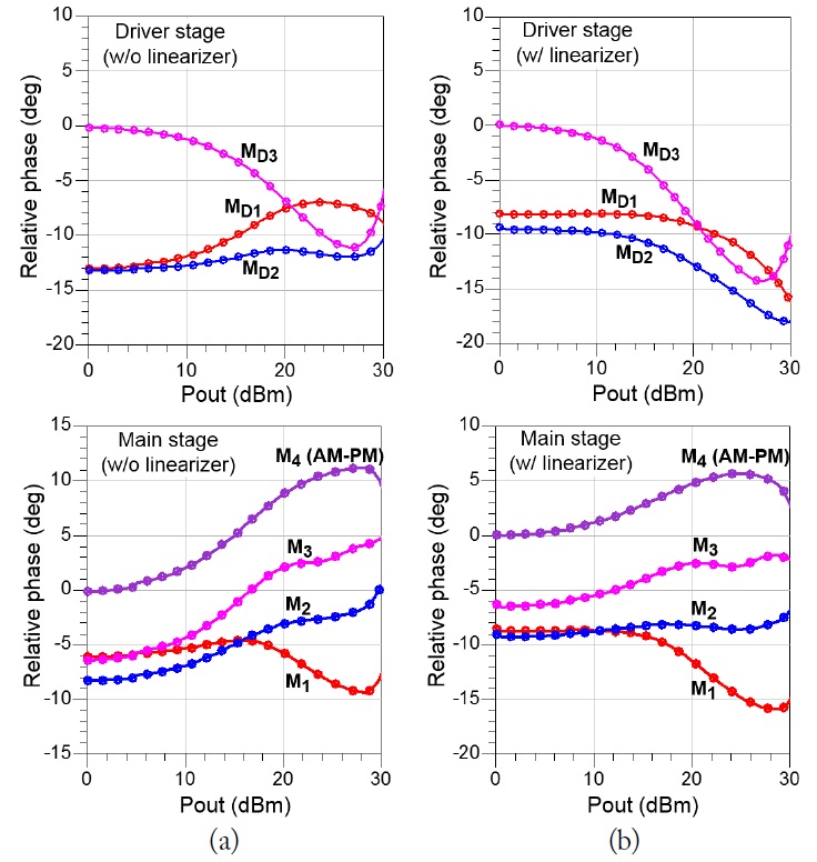
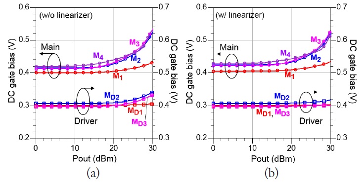
In addition, investigating the phase deviation by each FET of both stages is worthwhile. Fig. 4 shows the simulated drain voltage phase deviation of each FET. Contrary to the result without a linearizer, the phase of driver-stage using the linearizer becomes more pre-distorted, and then the signal is delivered to the main-stage. The phase deviation slope by the main-stage is the opposite direction to the input signal, and thus the resultant AM-PM is improved. Note that the stacked-FET structure is capable of self-phase compensation, because the CS amplifier and CG amplifier have the opposite phase characteristics [8]. Fig. 5 shows the simulated DC gate-source bias of each FET, where no significant difference is observed between the PAs with and without linearizers.
Ⅲ. FABRICATION AND MEASUREMENT
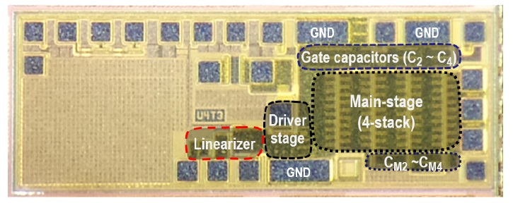
The designed linear PA was fabricated using a 0.18-μm silicon-on-insulator (SOI) CMOS process with high-resistivity substrate (
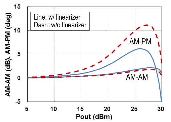
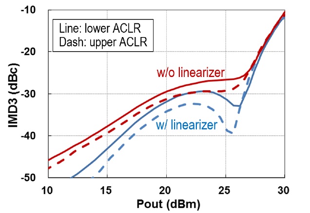
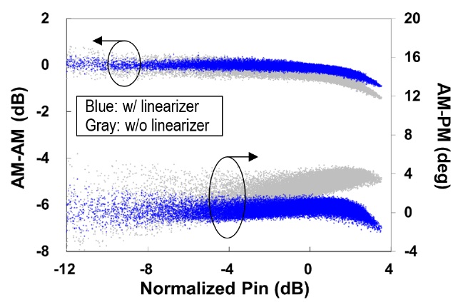
The implemented PA module was tested under the 3GPP uplink W-CDMA signal (Rel’99) at 836.5 MHz and a supply voltage of 4 V. The idle current is 75 mA. Prior to the W-CDMA test, the nonlinear characteristics of the PA were measured using single-tone (continuous wave [CW]) and two-tone signals. Fig. 7 shows the measured AM-AM and AM-PM characteristics using a CW signal. The AM-PM deviation of the linearized PA was reduced from 11.5° to 6°, which is close to the simulation result. Fig. 8 shows the two-tone third-order inter modulation distortion (IMD-3). By employing the linearizer, the linear output power meeting IMD3 = -30 dBc is extended.
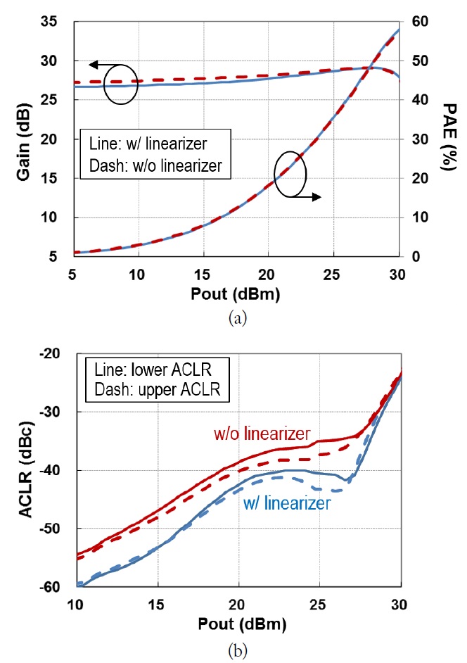
The measurement results of power gain, power-added efficiency (PAE), and adjacent channel leakage ratio (ACLR) using W-CDMA signal are plotted in Fig. 9. The PA showed a power gain of higher than 27 dB and ACLR better than -40 dBc up to the output power of 27.1 dBm. Output powers / PAEs meeting ACLRs of -40 dBc and -36 dBc were 27.1 dBm / 45.6% and 27.7 dBm / 48.3%, respectively. Compared to the reference PA without a linearizer, which showed ACLR of -36 dBc and PAE of 38.5% at
[Table 1.] Performance comparison of recently reported W-CDMA CMOS power amplifier
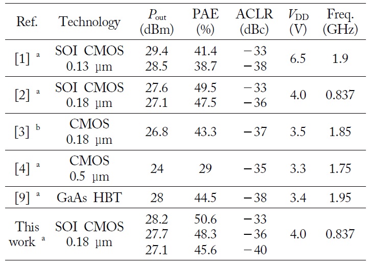
Performance comparison of recently reported W-CDMA CMOS power amplifier
The performance of the recently reported W-CDMA PAs is summarized in Table 1 for comparison. The linearity and efficiency of the proposed PA is favorable among the reported PAs. Its performance is also comparable to the Ga-As-based PA [9].
A linear stacked-FET PA module has been implemented using SOI CMOS technology for W-CDMA handset applications. The gate-source capacitance nonlinearity of a common-source amplifier is compensated by employing a PMOS linearizer with optimized phase (capacitance) slope at the gate of the driver-stage transistor. Thus, the AM-PM is improved while avoiding capacitance overloading effect at the main-stage. The fabricated PA showed PAE of 45.6% and meets the UMTS linearity requirement with margin (< -40 dBc versus system spec of -33 dBc) at