Wireless power transmission (WPT) technology is being spotlighted as high power transmission [1]. Short range transmission has been researched by studies on inductive coupling and resonant coupling methods. However, the transfer ranges of these technologies are limited to a few centimeters to a few meters [2]. Recently, long range WPT technology using microwave radiation methods has been investigated on the strength of advances in high power radio-frequency (RF) sources and the Schottky diode [3,4]. Unlike energy harvesting, which converts a small signal to direct current (DC) power, WPT deals with high power at the receiving system and the operating frequency is generally high to obtain a high gain for the antenna system [5]. Thus, the design parameters of a rectifier for use in a WPT system at high frequency region differs from those use for low frequency or baseband rectifiers. Typically, a Schottky barrier diode is used for a RF rectifier due to its fast switching speed [6]. However, as the frequency increases, the maximum breakdown voltage of the Schottky diode is reduced. Consequently, this leads to a low output DC voltage as well as a low system power capacity [7]. Furthermore, a typical WPT system consists of an antenna array that delivers high power to the rectifier circuit. Therefore, designing a high frequency rectifier system with greater power capacity that can produce both high output DC voltage and high conversion efficiency at a high power is the key factor in the fabrication of the receiving system of a high frequency WPT system.
This paper is focused on improving the power capacity of the rectifier system by using a Greinacher voltage multiplying circuit. This voltage multiplying circuit is made up of many lumped capacitors that are put between diodes [7]. However, the use of a lumped capacitor is difficult at high frequency due to its self-resonant frequency (SRF). The use of a Greinacher voltage multiplier circuit at high frequency first requires analysis of the I-V characteristics of the Schottky barrier diode.
Every simulation and measurement in this paper is conducted using Avago Technologies HSMS-8101 and HSMS-8202 Schottky barrier diode. The substrate is Taconic TLC-30-0200, which has a permittivity of 3.0 and 0.003 of tangent loss at 10 GHz. A single tone signal in the X-band is used as the experimental frequency.
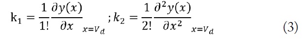
Ⅱ. RECTIFIER WITH MULTIPLE DIODES
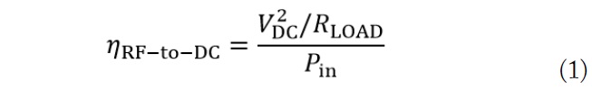
A rectifier converts time-varying power to DC power. One of the figures of merit of the RF rectifier is its RF-to-DC conversion efficiency, which is determined by following equation [1]:
The rectification process in the high power RF band differs from a baseband rectifier. First, most of the diodes used in RF rectifiers are Schottky diodes. The Schottky diode has a fast enough switching speed to rectify an RF signal. However, the Schottky diode has a low peak inverse voltage (PIV), so it is not practical for use in high power applications [7]. Although the Schottky diode has a low PIV and worse power handling capacity than a PN junction diode, its fast switching speed is essential for an RF rectifying system.
Secondly, the matching point varies with the input power. Power source impedance should equal the complex conjugate of the input impedance of the RF circuit. However, since the input impedance of these nonlinear circuits, including the Schottky diode, significantly changes with the input signal level, obtaining a conjugate impedance match is difficult for all input power in the WPT system. Typically, these circuits are designed for a specific value of input power level, mostly the primary operating input power level expected for the circuit [3]. Thus, the choice of an appropriate input power is a very important design factor. An input power range that exceeds the desired RF-to-DC conversion efficiency is another figure of merit of a large signal rectifier. Each element in a WPT system gets a different power due to nonuniformity of the main lobe of transmitter; therefore, the center of the receiving array and the edge of the receiving array get very different power.
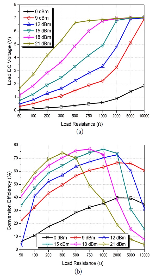
Fig. 1 shows the maximum load DC voltage and conversion efficiency for a Greinacher voltage doubler versus the load resistance for each input power. This simulation is conducted under ideal input and output matching. The harmonic generated by the nonlinear Schottky diode is not considered. As shown in Fig. 1(a), the output DC voltage produced by high load resistance is limited by the breakdown effect of the Schottky diode. In this paper, the use of the Avago HSMS-8102 Schottky diode results in a 7.0 V of saturated output DC voltage for the Greinacher voltage doubler from 9 dBm of input power. However, the load resistance for each saturation point of input power differs from each other, as shown in Fig. 1. Thus, the load resistance and input power must be tuned for the best performance of a given WPT system.
Ⅲ. HIGH FREQUENCY RECTIFICATION PROCESS
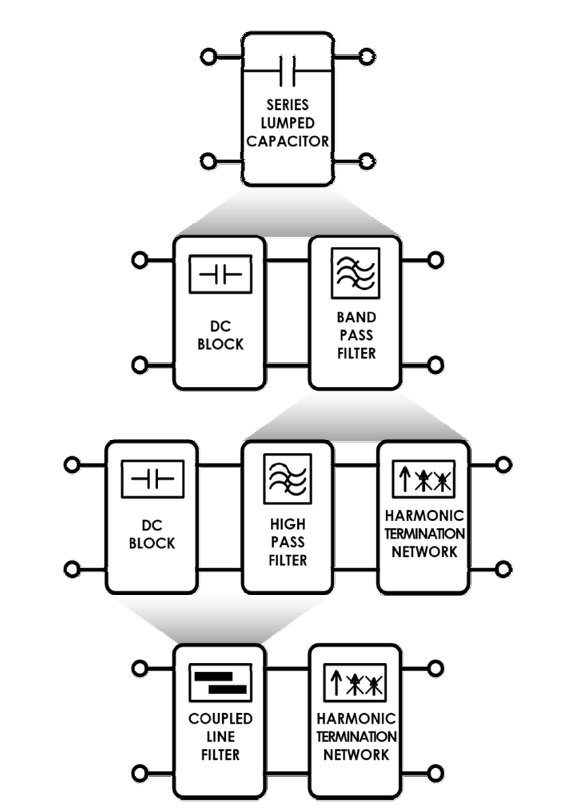
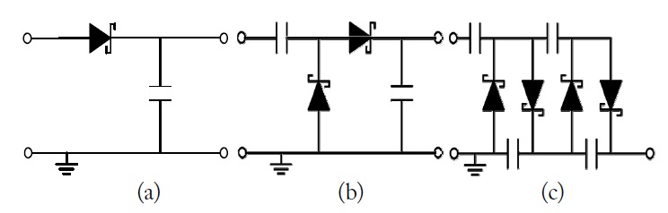
Fig. 2 shows a conventional halfwave rectifier and Greinacher voltage multipliers. These conventional circuits contain one or more lumped capacitor. However, the use of a lumped capacitor is difficult at high frequency due to its SRF. Hence, the high frequency rectifier needs an equivalent circuit for the lumped capacitor. Some of the lumped capacitors can also be omitted at high frequency.
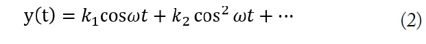
Lumped capacitors are classed as shunt capacitors and series capacitors. Shunt capacitors are omitted by the I-V characteristics of the Schottky diode. In general, for the rectifier that rectifies only a single tone signal, the power series expansion method is used to obtain the output current. The output current
The role of the shunt capacitor of the rectifier that uses a PN junction diode at a low frequency is charging, and for the mixer, the role of the shunt capacitor is as an envelope detector or low pass filter (LPF). For the rectifier using the Schottky diode, the charging mechanism is not needed due to its linear I-V characteristic in the operating region.
Eq. (2) can be modified as follows [8]:
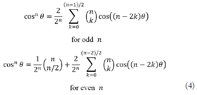
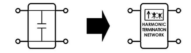
Eq. (4) shows that the output current of the Schottky diode is divided into a DC part and a harmonic part. If LPF is used to eliminate this time varying power (that is, the harmonic termination network), only DC power remains; thus, the rectification process occurs. Fig. 3 shows the substitution of the harmonic termination network for a shunt capacitor [9].
The equivalent circuit model for a series capacitor is the high pass filter (HPF). However, the series capacitor used in the Greinacher voltage multiplier circuit acts as both an HPF and also a DC block (DCB) for DC bias. That is, unlike the shunt capacitor, which acts as a simple LPF, the series capacitor acts as a charging capacitor. Moreover, for the series capacitor at the input network, the operating frequency surpasses this and should block higher order harmonics as well as the DC at the same time. Therefore, the series capacitor should act as a band pass filter (BPF) and a DCB. However, realizing both the BPF and DCB at the same time is difficult, especially at a high frequency. Therefore, in this paper, the high order harmonics are terminated by an additional input harmonic termination network. As a result, the series capacitor acts as an HPF and a DCB. An additional network, such as a harmonic termination network, is also added to the HPF to realize BPF. HPF is realized using a simple coupled line filter, which also acts as a DCB [10]. These procedures are summarized in Fig. 4.
Ⅳ. HIGH FREQUENCY GREINACHER VOLTAGE MULTIPLIER
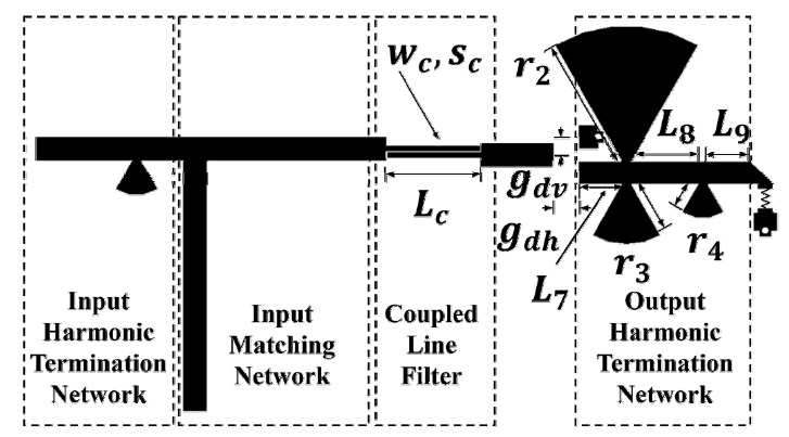
The designed Greinacher voltage multipliers are shown in Figs. 5 and 6. The input network of these rectifiers consists of a matching network and an input harmonic termination network. There is a via at the input harmonic termination network of the halfwave rectifier [3]. The role of this via is to eliminate the reflected DC harmonic caused by the nonlinear characteristics of the Schottky diode. However, for the Greinacher voltage multipliers, unlike the halfwave rectifier, the DCB moves from the foremost of the input network to the very end of the input network; that is, right in front of the diode. This is because the DCB act as an HPF, as shown in Fig. 4. This DCB is designed for passing the operating frequency and it blocks DC. Input high order harmonics are eliminated at the input harmonic termination network. Unlike the input harmonic termination network in a halfwave rectifier, the Greinacher voltage multiplier does not need a via through the ground. The reflected DC harmonic caused by the diode is blocked by a coupled line filter right in front of the diode. This makes a simpler input network than that of the halfwave rectifier. The DCB at the foremost of the input network is needed to prevent the via from affecting the receiving antenna or the signal source.
The conventional Greinacher voltage doubler and quadrupler are shown in Fig. 2(b) and (c) [11]. A high frequency, capacitorless Greinacher voltage doubler can be designed by replacing the series capacitance with HPF and DCB, and the shunt capacitance with LPF. The output network of the designed rectifier consists of an output harmonic termination network and a load resistance. Since the input matching network is dramatically changed by the output network, the output network is the most important. Notably, the fundamental frequency must be eliminated at the output network. The fundamental frequency component is predominant when the input power is high. If the fundamental frequency and other higher order harmonics are not eliminated, the output DC voltage will be degraded by ripple and the DC voltage also cannot be measured. The output harmonic caused by the diode must be eliminated as near as possible to the diode. The shorter the
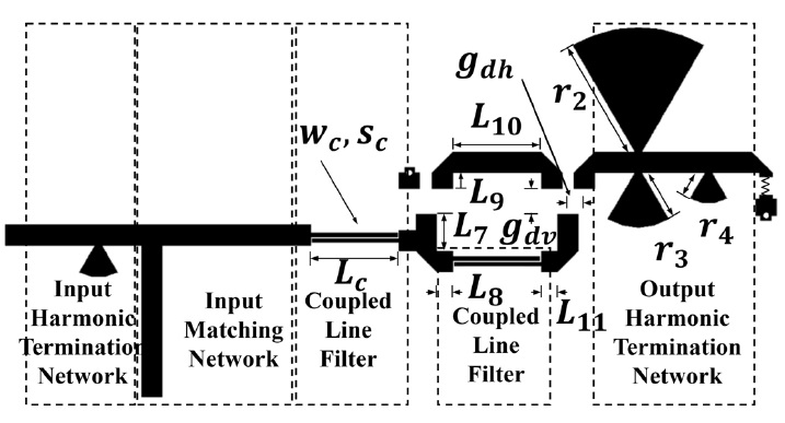
The output network of the Greinacher voltage quadrupler consists of an output harmonic termination network and a load resistance. Like the Greinacher voltage doubler, the shorter the
[Table 1.] Specific values of the designed high frequency Greinacher voltage doubler
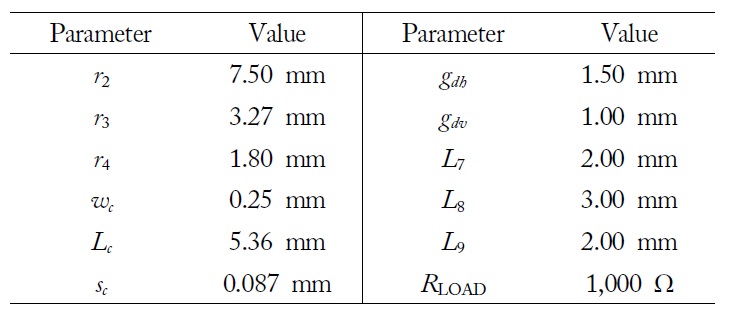
Specific values of the designed high frequency Greinacher voltage doubler
[Table 2.] Specific values of the designed high frequency Greinacher voltage quadrupler
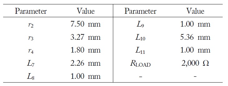
Specific values of the designed high frequency Greinacher voltage quadrupler
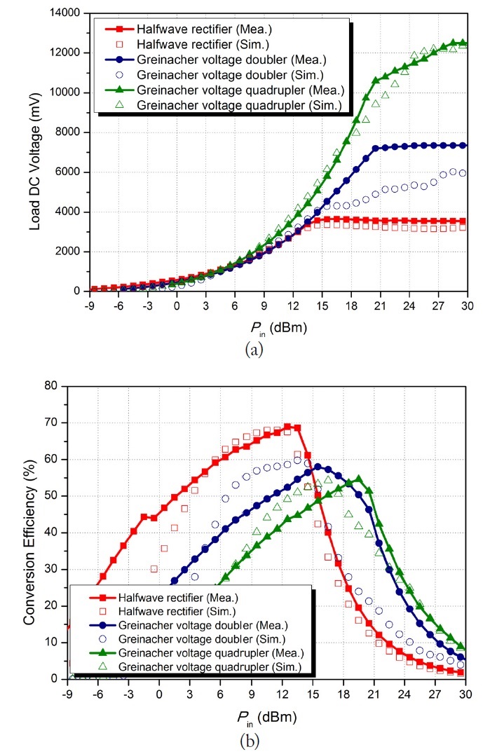
Fig. 7(a) shows the output DC voltage for the three types of rectifiers, while Fig. 7(b) shows the conversion efficiency. As diodes double, the power handling capacity also increases by 3 dB and this is shown in both Fig. 7(a) and b). The peak point of conversion efficiency occurs when the input power is 13, 16, and 20 dBm for the halfwave rectifier, Greinacher voltage doubler, and quadrupler, respectively. The breakdown voltage is the main parameter that controls the power handling capacity of the rectifier and it can be increased by placing multiple diodes. Multiple diodes consume excited power equally; therefore, the overall power handling capacity of the rectifier system increases. As the power handling capacity is increased by 3 dB for each other, the peak point of conversion efficiency also varies by 3 dB, as shown in Fig. 7(b). However, the Greinacher voltage multiplier does not always multiply the output voltage but multiplies the saturated voltage. This phenomenon is seen in Fig. 7(a) and is due to the DC component generated from the Schottky diode. For the halfwave rectifier, this generated DC component is eliminated by a grounded stub. However, for the Greinacher voltage multiplier, the DCB blocks the generated DC component, thereby lowering the self DC bias in front of the diodes.
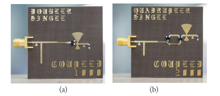
The results show that a halfwave rectifier, which is a reference rectifier, shows 3.55 V of saturated voltage and 69% of maximum conversion efficiency at 12.5 dBm of input power. The optimal load resistance for a halfwave rectifier is 745 Ω. The Greinacher voltage doubler shows 7.35 V of saturated output DC voltage and shows 58% of maximum conversion efficiency at 15.5 dBm of input power, which is 3 dB higher than that of the halfwave rectifier. The optimal load resistance for the Greinacher voltage doubler is 997 Ω. The Greinacher voltage quadrupler shows 12.50 V of saturated output DC voltage and shows 55% of maximum conversion efficiency at 19.5 dBm, which is 7 dB higher than that of the halfwave rectifier. The optimal load resistance for the Greinacher voltage quadrupler is 1,950 Ω. Resistance values are measured values and fabricated circuits are shown in Fig. 8. Degradation of the maximum conversion efficiency is due to a generated DC component.
The use of the distributed Greinacher voltage multiplier increases the power handling capacity by about 3 dB by doubling the number of diodes. As more rectifiers are increasingly doubled, the optimal resistance for maximum conversion efficiency is increased. The research presented here indicates that the proposed distributed Greinacher voltage multiplier can be applied to high power WPT systems. The measurement results are similar to method of moment simulation results, and the tendency is pronounced.