The demand for multi-gigabit data transfer over a wireless link is expediting the advent of millimeter-wave applications (30 to 300 GHz) [1]. In virtue of a shorter wavelength compared to the microwave frequency, a much broader bandwidth can be obtained with physically smaller electronic components, such as waveguides, cavities, and antennas. One promising application utilizing the millimeter-wave band is chipto-chip communication [2]. A wireless link between electronic chips may reduce the portion of wired connections, for instance, bonding wires, ball grids, and printed circuit board (PCB) traces, resulting in better manufacturability and less dissipation loss in high data rate communication.
In this letter, we report a novel PCB-embedded antenna for millimeter-wave chip-to-chip communication. The antenna is designed to operate in the frequency band of 76 to 84 GHz and to radiate horizontally to the PCB surface. It is extremely low profile as the height of the antenna is only 0.18 mm, which is 0.05
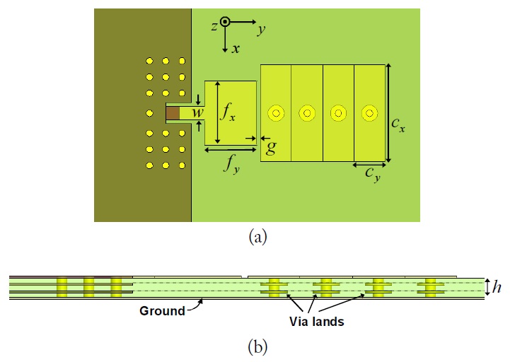
Fig. 1 depicts the top and side view of the proposed antenna. As mentioned, the antenna height is restricted to
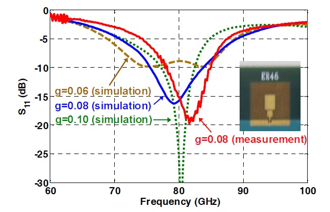
Parametric studies based on a full-wave simulation tool (Ansys high-frequency structure simulator [HFSS]) show that the antenna resonance frequency and bandwidth can be tuned by the parameters
The optimized antenna design is carried out with
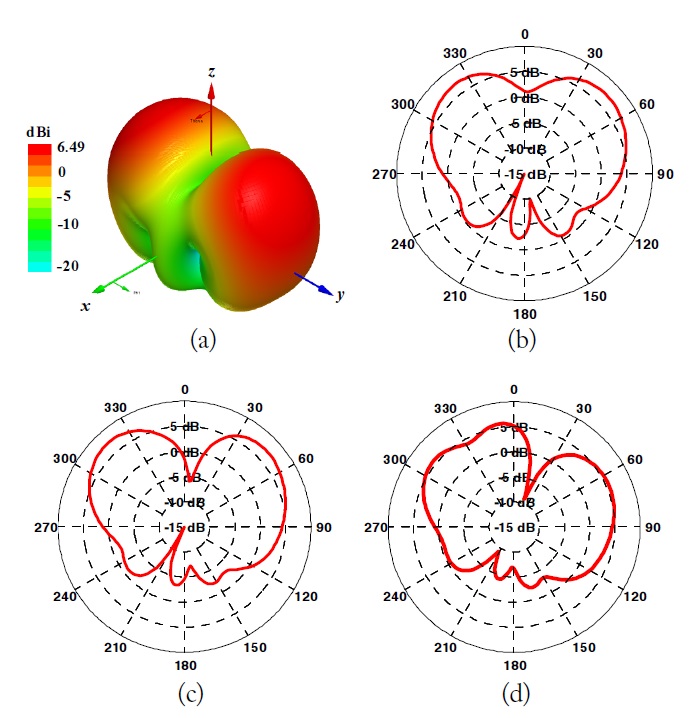
Fig. 3(a) depicts the simulated three-dimensional (3D) radiation pattern of the optimized design at 80 GHz. A "butterfly-like" radiation pattern is observed. This unique pattern originates from the combination of two different radiation modes: the zeroth- and first-order modes. They exhibit a monopole-like and patch-like radiation pattern, respectively. Their combination makes a null not only in the z-di rection but also in the x-direction, resulting in the butterfly- like radiation pattern. Successive 2D plots in Fig. 3(b)-(d) refer to the yz-cut of the radiation pattern at 76, 80, and 84 GHz, respectively. As can be seen, the butterfly-like pattern remains throughout the bandwidth in that the proposed antenna not only provides a consistent matching condition but also a radiation pattern. Note that the butterfly-like radiation pattern is somewhat deformed at 84 GHz, implying the first-order mode starts to become dominant over the zeroth-order mode. Although a maximum gain of 6.5 dBi occurs at
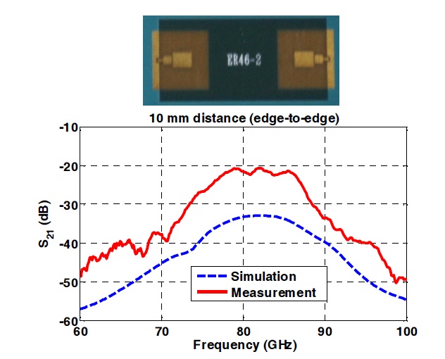
Having verified that the proposed antenna successfully delivers the radiated energy alongside the PCB surface, we proceed to measure the transmission coefficient (S21) between two antennas. Fig. 4 shows the fabricated test configuration together with the simulation and measurement results of S21. The two antennas face each other with an edge-to-edge distance of 10 mm. Based on a link budget analysis, S21 > -40 dB guarantees reliable chip-to-chip communication over a 10-mm range. As observed in the figure, the simulated S21 ranges from -36.6 to -32.9 dB at 76 to 84 GHz, satisfying the above requirement. The measured data exhibit a similar trend as the simulation but with a much higher S21 value, from -25.3 to -20.8 dB. The reason for this 10-dB difference is that the GSG probe mount behind the antenna feed acts as a reflector, therefore, the backward radiation adds up to the forward radiation.
A millimeter-wave PCB-embedded antenna is presented for use in chip-to-chip communication. A metamaterial-inspired ZOR antenna design technique is employed to avoid radiation vertically to the ground while keeping the antenna at an extremely low profile. Simulation and measurement results demonstrated that more than 10% of the bandwidth can be covered by optimizing the microstrip stub feeding section. It further provides a distinctive butterfly-like radiation pattern suitable for wireless communication along the PCB surface.