Cadmium sulfide (CdS) thin films have been used for CdS/CdTe and CdS/CuInSe2 solar cells [1-4]. CdS thin films are prepared by vacuum evaporation [2,4], sputtering [1,5], screen printing [4], chemical spray [6], and chemical bath deposition(CBD) [2-4,7]. The CBD method is based on a controlled precipitation of the material in such a way that the precipitation occurs uniformly onto the substrate [7]. In addition, film formation on the substrate takes place when the ionic product exceeds the solubility product [8].
Regarding the chemical processes of CdS thin films by CBD,the heterogeneous reaction on the substrate surface is limited by the competing homogeneous reaction in solution (which results in precipitation in solution) [9]. Nanocrystalline semiconductors exhibit properties that intermediate between the bulk crystals and the molecules [10]. Nanocrystalline CdS thin films are grown on substrates in a solution bath containing cadmium salt and a complexing agent. One of the cadmium salts, either cadmium chloride, cadmium acetate, or cadmium sulfate is used. Wenyi et al. [11] reported on the influence of the growth process on the structural, optical, and electrical properties of CBD CdS films.The surface morphology, structural, and optical properties of CdS thin films depend on the deposition parameters, notably the concentration of the reactants, the pH of the solution, the bath temperature, and the deposition time.
In this study, CBD was used to deposit nanocrystalline CdS thin films onto glass substrates. The CdS thin films were characterized using X-ray diffraction (XRD), photoluminescence (PL),and the temperature dependence of the PL intensity fitted with theoretical expression. Also, the Fourier transform infrared spectroscopy(FTIR) results for the CdS thin films are reported.
2.1 Deposition of the CdS thin films
The glass slides were washed in distilled water and ultrasonically subsequently cleaned in acetone, trichloroethylene (TCE), and methanol. The substrates were then rinsed in deionized water,blown with N2, and dried in an oven. In order to prepare the reaction solution, 25-28% NH4OH was added to a bath of 0.5 M CdSO4 aqueous solution; 1 M thiourea was then added to this solution bath. The S2- ions are provided by the dissociation of thiourea in an alkaline medium, and react with the Cd(NH3)4 2 ions to form CdS thin films [12]. The CdS thin films were prepared on glass substrates in the chemical bath at 80°C with a pH of 10 using different times varying from 30 to 120 min. The deposited CdS thin films were rinsed in deionized water and cleaned ultrasonically.The CBD CdS films were then dried in air. The CdS thin films are yellowish and have a good adherence to the glass substrate.
2.2 Characterization of the CdS thin films
In order to measure the thickness of the CdS thin films, an ellipsometer(L116SF; Gaertner Scientific Co., Skokie, IL, USA) was used. The surface morphology of the CdS thin films was studied using field emission scanning electron microscopy (FE-SEM)(JSM-6700F; Jeol Ltd., Tokyo, Japan). The crystal structure was characterized by XRD, using a X-ray diffractometer (X��pert-APD;Philips, Netherlands) using Cu Kα radiation (λ = 1.5406 Å). The PL emission spectra were obtained using a spectrometer (f=0.5 m, Spectrograph 500i; Acton Research Co., Acton, MA, USA) and an intensified photodiode array detector (IRY1024; Princeton Instrument Co., Trenton, NJ, USA). A He-Cd laser (1K; Kimon,Japan) with a wavelength of 325 nm and a power of 50 mW was used as the excitation source. The temperature dependence of the PL intensity for the CdS thin films was studied from 16 to 300 K. To study the presence of impurities, a FTIR analysis using the attenuated total reflectance mode was carried out using a spectrophotometer (Nicolet 6700; Thermo Fisher Scientific Inc.,Madison, WI, USA) in the range of 400-4,000 cm-1.
The chemically deposited CdS thin films were uniform and consisted of small nanocrystalline grains. The preparation of CdS thin films by CBD is governed by the chemical reaction within the solution of reactants. It was reported that at lower temperatures the surface of the CBD CdS thin films is rough, but as the temperature continues to increase (at 80℃), the film surface becomes more uniform [13].
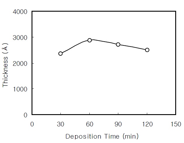
Figure 1 shows the variation of the CdS film thickness according to the deposition time. It reaches a maximum at the deposition time of 60 min and then decreases as the deposition time increases. This trend in the CdS thickness is analogous to the results of Lokhande et al. [14]. After a certain deposition time, the desorption and/or the dissolution process predominates over the heterogeneous and homogeneous precipitation, resulting in a decrease in the film thickness [8].
The as-deposited CdS thin films were crystallized. The three diffraction peaks correspond to the (111), (220), and (311) reflections of the cubic phase at a 2 0.9 cos Dλβ θ=of 26.5°, 44°, and 52° respectively.On the other hand, the lattice constant of the CdS thin film deposited at 80°C for 60 min was 5.81 Å.
The crystallite size of the CBD CdS thin films is affected by deposition conditions. It is useful to obtain the information of the structural properties of the thin films by XRD measurement. The crystallite size
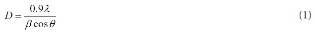
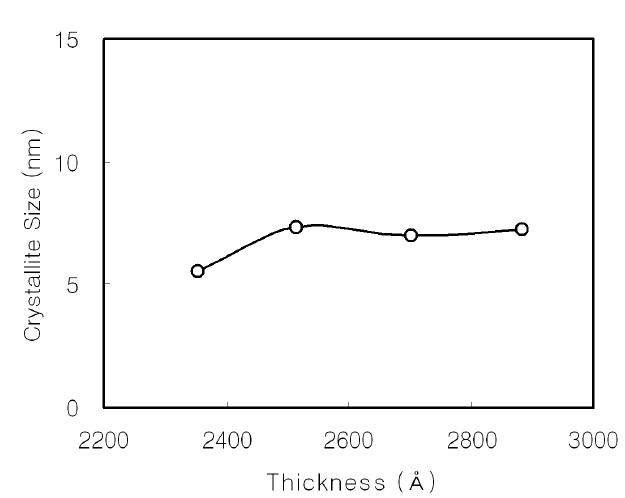
The crystallite size was calculated using the FWHM value from the XRD measurement. Figure 2 shows the crystallite size of the CdS thin films as a function of the film thickness. It initially increases as the film thickness increases, and it is nearly constant at about 7 nm over a thickness of 2,500 Å.
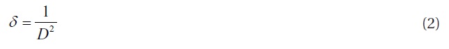
where D is the crystallite size of the CdS thin film.
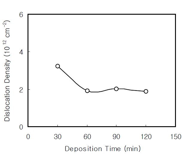
Figure 3 shows the dislocation density of the CdS thin films as a function of the deposition time. The dislocation density initially decreases as the deposition time increases. The dislocation density has a small variation above 60 minutes and is nearly constant.This result confirms that the CBD reaction is stable above 60 minutes.
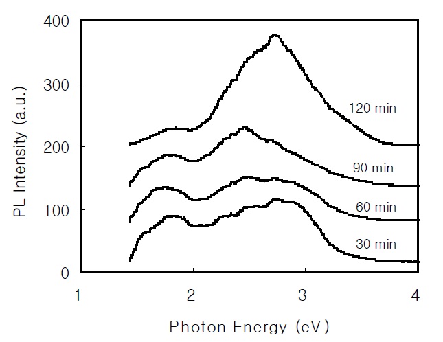
The PL spectrum is used to study the optical properties of thin films. Figure 4 shows the PL spectra of the CdS thin films at room temperature. The broad red band around 1.7 eV and the broad high-energy band around 2.7 eV are attributed to the S vacancy(VS) and the band-to-band transition, respectively.
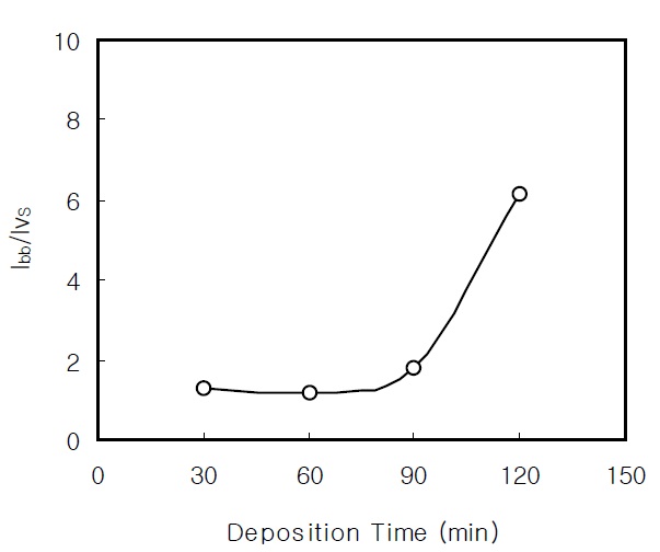
The band-to-band transition energy is confirmed in the PL spectra. The band gap energy of the CdS thin films is nearly the same as the result from the transmittance measurement. The PL intensity ratio Ibb/Ivs of the nanocrystalline CdS thin films between the two bands is shown in Fig. 5. As the deposition time increases to over 90 min, the PL intensity from the band-to-band transition significantly increases. The increase of the Ibb/Ivs is caused by the improvement of the crystalline quality of the CBD CdS thin films [17].
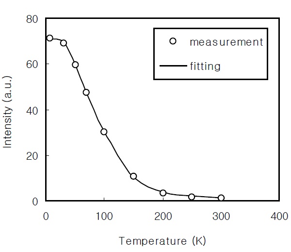
In order to obtain the activation energy of the CdS thin films, it is necessary to investigate the temperature dependence of the PL intensity. Figure 6 shows the temperature dependence of the PL intensity for the CdS thin film prepared for 60 minutes. This was compared with the fitting result of the theoretical expression; the two regions were confirmed. The temperature dependence of the PL intensity was fitted using the following equation [18]:
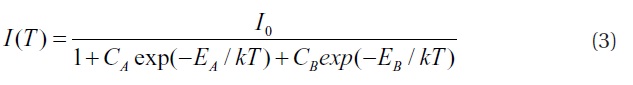
where EA and EB are the activation energies, CA and CB are the fitting parameters, and
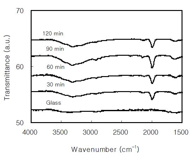
The FTIR spectra of the CdS thin films are shown in Fig. 7. A broad absorption band in the range from 3,000-3,600 cm-1 and a small band around 1,610 cm-1 are due to the OH stretching vibration of the water molecules [19]. The peak at 2,000 cm-1 is attributed to the CN stretching vibration of cyanamide or thiocyanate, which a result from the chemical reaction of the thiourea and ammonia [20].
Nanocrystalline CdS thin films were prepared on glass substrates by CBD using an alkaline solution. The CdS thin films were investigated using XRD, PL, and FTIR. The crystallite size of the CBD CdS thin films initially increased as the film thickness increased; it was nearly constant as about 7 nm over the thickness of 2,500 Å. In addition, the dislocation density initially decreased as the deposition time increased, and showed a small variation above 60 min, then remained nearly constant.
In the PL spectrum of the 2,900 Å-thick CdS thin film, the broad red band around 1.7 eV and the broad high-energy band around 2.7 eV are attributed to the S vacancy and the band-toband transition, respectively. By fitting the temperature dependence of the PL intensity, the activation energies of the EA and EB of the CdS thin film prepared for 60 min were 63.7 meV and 13.7 meV, respectively. From the FTIR analysis of the CdS thin films,a broad absorption band due to the OH stretching vibration and the peak at 2,000 cm-1 due to the CN stretching vibration were found.
The XRD and PL were performed at the Korea Basic Science Institute (KBSI), and the FE-SEM and FTIR were conducted at the Center for Instrumental Analysis of Andong National University.