The integrated circuit industry is always under pressure to shrink down the device size while maintaining good performance and many studies have been performed to address associated problems. In CMOS technology, the development of highk materials, i.e. with a high dielectric constant (k), to address the current leakage problem has attracted a great deal of attention[1]. Concurrently, in mass storage memory devices, high-k dielectrics are also of great interest for applications driven by scaling [2]. According to the 2007 Edition of the International Technology Roadmap for Semiconductors (ITRSs), high-k materials will be introduced as a replacement for interpoly dielectrics in sub-28 nm NAND Flash technological nodes [3]. Among the various high-k materials, aluminum oxide (Al2O3) has the potential to be used for future generation devices due to its special physical and chemical properties [2]. With a k-value of ~10, large bandgap (~6.5 eV) and elevated crystallization temperature [4],Al2O3 has been studied as a main candidate to replace oxide nitride oxide (ONO) as the poly-Si dielectric (IPD) in floating gate devices or as the blocking oxide (BO) for charge trap memories[5,6].
Several etching techniques have been studied to obtain a high etch rate and etch selectivity. Among them, the inductively coupled plasma (ICP) system was employed in our experiments due to the good properties of the high-density plasma, easy control of the ion energy and flux, and simple structure. Various gases,such as BCl3, CCl4, SiCl4, HF, and CHF4 have been used to remove the native oxide (Al2O3) on the aluminum surface. The choice of BCl3 as the chemically active gas in the present study results from the fact that it is widely used for the etching of materials covered by native oxides due to its effective extraction of oxygen in the form of BClxOy compounds [7].
In this study, we used a BCl3/Ar inductively coupled plasma with additional O2 to etch the Al2O3 thin film. The etch rate and selectivity of Al2O3 over SiO2 were investigated as functions of the gas ratio, RF power, DC-bias voltage and process pressure. X-ray photoelectron spectroscopy (XPS) was performed to investigate the chemical reactions between the surface of the Al2O3 films and O2/BCl3/Ar plasma.
The Al2O3 thin films were etched by an ICP system. The substrates used were Al2O3 thin films deposited on a Si wafer using ALD. The thickness of the Al2O3 films was approximately 50 nm. The chamber was evacuated to a base pressure less than 1.3 ×10⁻⁴ Pa and then the etching gases were introduced. There was a gold-coated 3.5-turn copper coil on the top of the chamber separated by a 24 mm-thick quartz window. A 13.56 MHz RF power generator was connected through a matching network to the coil, in order to generate the plasma at the top of the process chamber. The wafers were placed on a chuck, which was used as the bottom electrode. The bottom electrode, which was used as the substrate holder, was connected to another 13.56 MHz asymmetric RF generator to apply a DC-bias voltage to the wafer.
In this experiment, the etching characteristics of Al2O3 as functions of the RF power in the range of 400-700 W, DC-bias voltage in the range of -50 to -200 V, process pressure in the range of 7.5-22.5 mTorr and gas ratio were investigated. The total flow of BCl3/Ar was fixed at 20 sccm. A surface profiler (KLA Tencor, astep 500) was used to measure the etch thickness. XPS was used to analyze the elements on the film surface. The samples were prepared to 1 cm × 1 cm without any pattern.
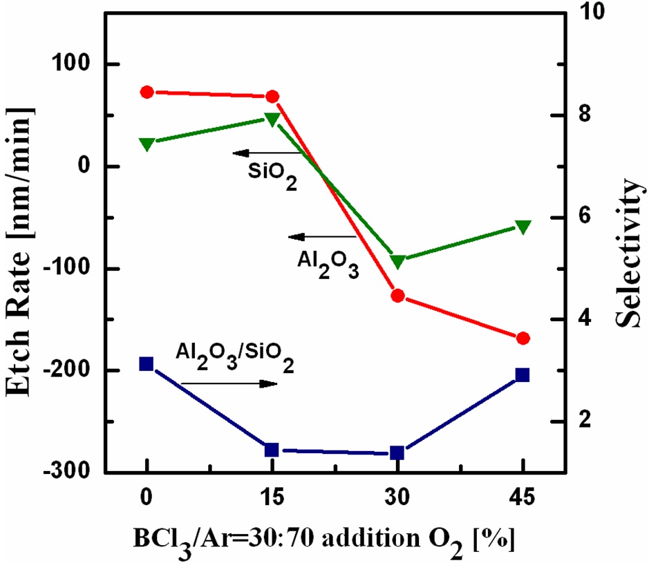
Figure 1 shows the etch rates of Al2O3 and SiO2, the selectivity of the Al2O3 film over SiO2 as a function of the gas ratio of O2 to (BCl3 Ar). The total flow rate of BCl3/Ar was fixed at 20 sccm and the flow rate of O2 was varied from 0 to 9 sccm. The RF power, DC-bias voltage, process pressure and substrate temperature were 500 W, -100 V, 15 mTorr, and 40℃, respectively. The BCl3 gas facilitated the extraction of oxygen in the form of BClxOy in the Al2O3 etching process. A high etch rate of 72 nm/min was obtained at O2/BCl3/Ar = 0/6/14. When 15% O2 was added to the BCl3/Ar gas, the etch rate was approximately 68.4 nm/min. Continually increasing the gas ratio of O2 caused heavy deposition,inhibiting the etching process on the surfaces of Al2O3 and SiO2. BCl3 is highly reactive and a good at acquiring oxygen can form nonvolatile residues upon contact with oxygen or water [8].One of the reactions between BCl3 and O is 2BCl3 + O → B 2O3 6Cl. The melting point of the byproduct B2O3 is as high as 450℃.When a small amount of O2 was added to the gas mixture, passivation layers of BxCly formed on the surfaces would be suppressed due to the concentration reduction of the inhibitor species BClx in the plasma through the formation of gaseous products via various reactions [e.g., 2BCl2 O → BOCl + BCl + 2Cl]. When an excessive amount of O2 was added to the gas mixture, thick layers of BxOy would be deposited on the surface due to the formation of solid products in the plasma [e.g., 2BCl3 3O �� B2O3 6Cl][9]. The highest selectivity of Al2O3 with respect to SiO2 of 3.1 was obtained at O2/BCl3/Ar = 0/6/14.
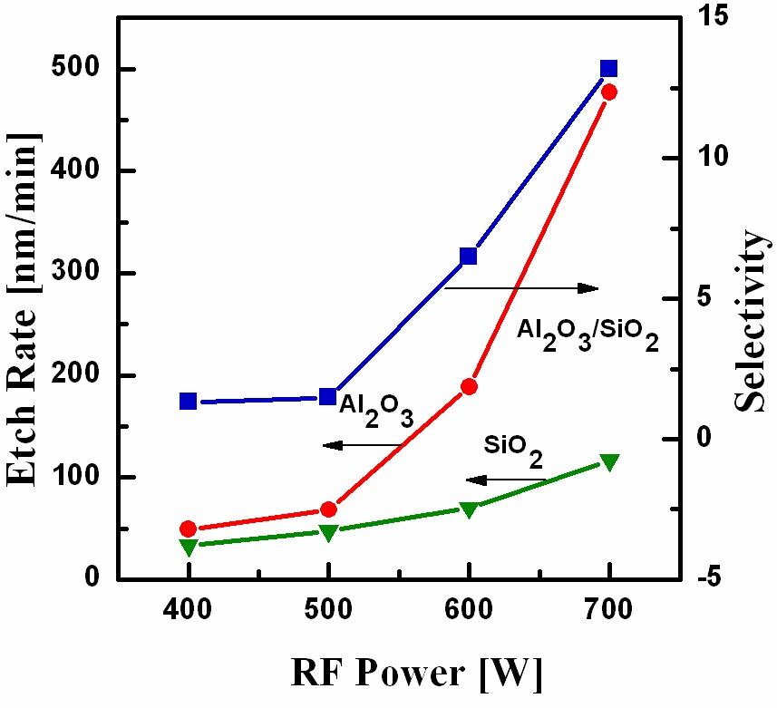
Figure 2 shows the etch rates of Al2O3 and SiO2 and the selectivity of the Al2O3 thin film with respect to SiO2 as a function of the RF power in the range from 400 to 700 W, while the other parameters were O2/BCl3/Ar = 3/6/14, a DC-bias voltage of -100 V, and a process pressure of 15 mTorr. Figure 2 illustrates the monotonic increase of the etch rate with increasing RF Power.A high etch rate of 477 nm/min was obtained at an RF power of 700 W and SiO2 also showed the same trend with a high etch rate of 36 nm/min obtained at an RF power of 700 W. The increase in etch rate could be explained by the fact that with increasing RF power, the plasma density increased due to the increase in the number of reactive free radicals and ions. Thus, enhancing the etch rates of Al2O3 and SiO2[10]. The acceleration of the chemical reactions as well as that of the physical ion bombardment occurred simultaneously. The selectivity of Al2O3 with respect to SiO2 showed a monotonic increase in Fig. 2. A high selectivity of 13 was obtained at an RF power of 700 W.
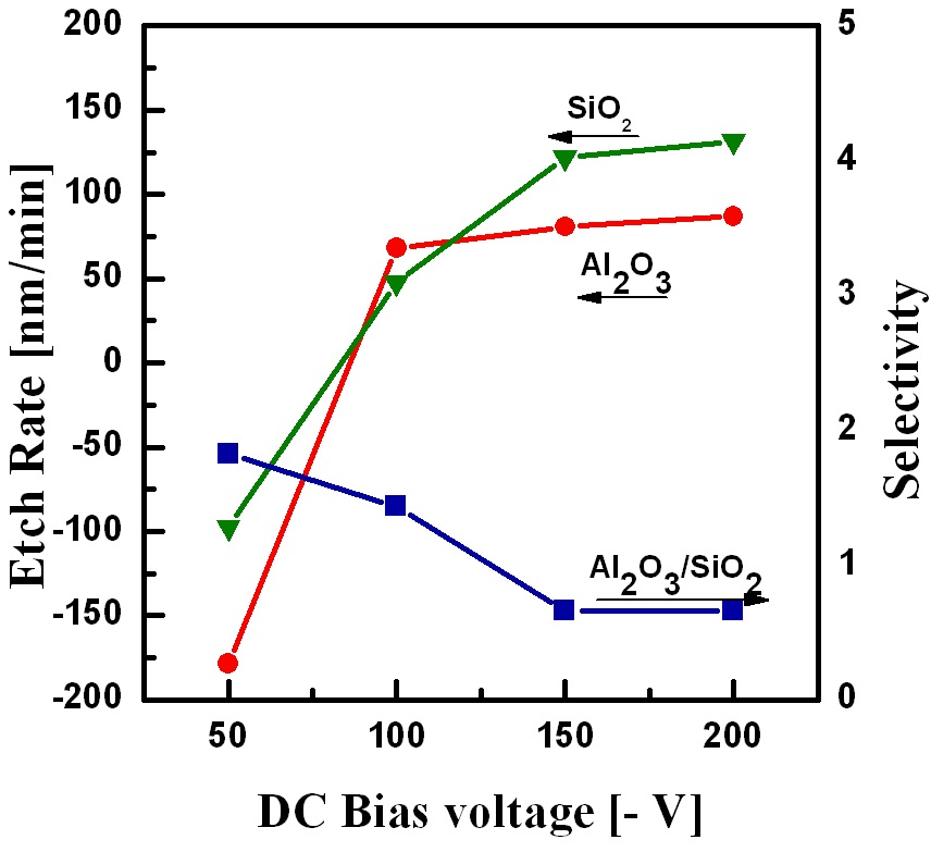
Figure 3 shows the etch rates of Al2O3 and SiO2 and selectivity of the Al2O3 film with respect to SiO2 as a function of the DC-bias voltage in the range from -50 to -200 V, while the other parameters were O2/BCl3/Ar = 3/6/14, an RF power of 500 W, and a process pressure of 15 mTorr. As shown in Fig. 3, when the DC-bias voltage increased from -50 V to -200 V, the etch rates on Al2O3 and SiO2 increased. According to this trend, high Al2O3 and SiO2 etch rates of 87 nm/min and 131 nm/min, respectively, were obtained at a DC-bias voltage of -200 V. With increasing DC-bias voltage,the self-bias applied to the samples and the kinetic energy of the impinging ions increased [11,12]. At a DC-bias voltage of -50 V,deposition occurred on the Al2O3 and SiO2 surfaces. A low DCbias voltage led to ions with a low energy being drawn onto the film surface, which could not remove the less volatile byproducts through physical sputtering by ion bombardment. As shown in Fig. 3, the DC-bias voltage had a greater influence on SiO2 than on Al2O3, which caused the selectivity of Al2O3 with respect to SiO2 to decrease. A high selectivity of 1.8 was obtained at a DCbias voltage of - 50 V.
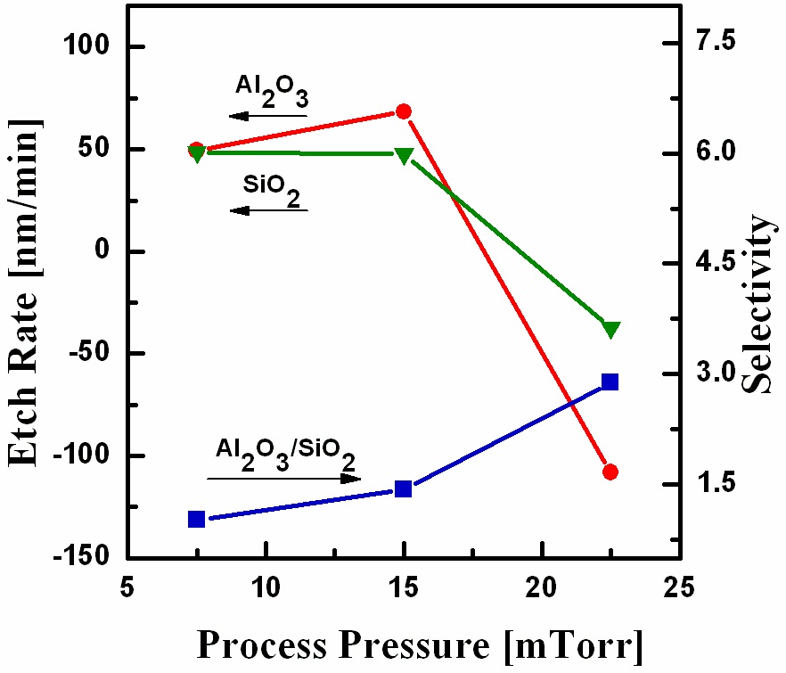
Figure 4 shows the etch rates of Al2O3 and SiO2 and the selectivity of the Al2O3 film with respect to SiO2 as a function of the process pressure in the range from 7.5 mTorr to 22.5 mTorr, while the other parameters were O2/BCl3/Ar = 3/6/14, an RF power of 500 W and a DC-bias voltage of -100 V. As shown in Fig. 4, the etch rate increased when the process pressure was increased from 7.5 mTorr to 15 mTorr, but deposition occurred on both Al2O3 and SiO2 when the process pressure was further increased to 22.5 mTorr. When the process pressure was too low, the gas would flow directly away, without participating in the etching process, thus causingrate to be lower. When the process pressure was increased,rate increased due to the increase in the density of the radicals. However, when the process pressure was increased beyond a certain threshold, deposition occurred on the surfaces. This could be explained by the fact that frequent scattering occurred, due to the shortening of the mean free path at the high process pressure, which accelerated the reactions between (boron - chloride) and oxygen, resulting in deposition. The selectivity of Al2O3 with respect to SiO2 increased and a high etch rate of 2.8 was obtained at a process pressure of 22.5 mTorr.
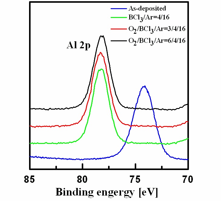
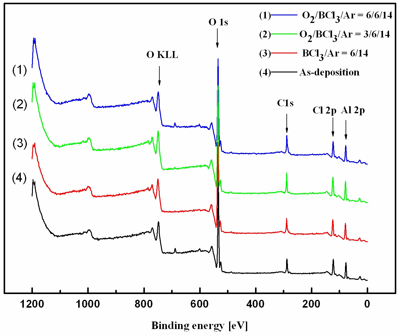
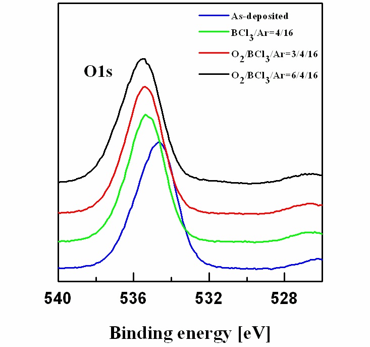
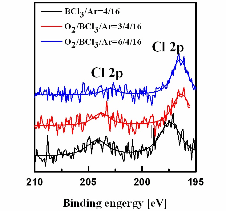
Figure 5 shows the wide-scan spectra obtained from the asdeposited and etched Al2O3 thin films surfaces. Figure 6 shows the narrow scan spectra of the Al 2p photoelectron peak, which were obtained from the as-deposited and etched Al2O3 thin films surfaces. The photoelectron peak at a binding energy of 74.3 eV corresponds to Al 2p of Al2O3. Compared with the spectrum of the as-deposited film, the Al 2p peak was shifted to 78 eV after etching, potentially due to Al-chlorine byproducts remaining on the surface after the reactions between Al and Cl. The O 1s photoelectron peaks are shown in Fig. 7. The O 1s photoelectron peak at a binding energy of 534.4 eV originated from the Al-O bonds in the as-deposited sample photoelectron peaks were shifted to 535-536 eV, possibly due to the B-O species from the boron-oxygen compounds BxOy deposited on the surfaces,which prevented the formation and sputtering of volatile byproducts[13]. Figure 8 shows the Cl 2p photoelectron peaks after etching in the BCl3-based gas mixture. The Cl that appeared on the etched surface may have originated from AlxCly compounds.The peaks of Cl 2p decreased as the amount of O2 increased. As the amount of O2 increased, more BCl reacted with the O radicals to produce nonvolatile byproducts, which led to less AlxCly being produced.
In this study, we investigated the etch characteristics of ALDdeposited Al2O3 thin films as functions of the amount of O2 in the BCl3/Ar plasma, RF power, DC-bias voltage and process pressure using an inductively coupled plasma system. As the RF power and DC-bias voltage increased, the etch rates of Al2O3 and SiO2 increased due to the increasing density of the radicals and kinetic energy of the ions. The highest etch rate of 477 nm/min was obtained at an RF power of 700 W with the addition of 15%O2 to the BCl3/Ar gas, a DC-bias voltage of -100 V and a process pressure of 15 mTorr. As the process pressure was increased, deposition occurred at a high process pressure, due to the frequent scattering which accelerated the reactions in the plasma. Since BCl3 is highly reactive and good at acquiring oxygen, it can form nonvolatile residues upon contact with oxygen or water. When a small amount of O2 was added, the concentration of the inhibitor species of boron chlorides in the plasma was reduced, suppressing the formation of a passivation layer on the surface. However,as the amount of O2 was increased, solid products consisting of boron oxides were formed in the plasma, resulting in heavy deposition on both Al2O3 and SiO2 surfaces.