ABO3 perovskite type lead zirconat titanate (Pb(Zr,Ti)O3 (PZT))is one of the most important electric materials for use in piezoelectric transducers such as buzzers, underwater sonar, speakers, ultrasound transducers for medical diagnostics, and actuators for precise positioning. The electrical conductivity of PZT ceramics can be controlled by minor modification of the dopants and by variation of the sintering conditions without seriously affecting the other properties. The large number of polarization directions available in PZT compositions near the morphotrophic phase boundary renders the solid solution of tetragonal PbTiO3 (PT) and rhombohedral PbZrO3 (PZ) easy to pole to a high remanent polarization [1]. In the poled state, PZT exhibits superior piezoelectric properties and a relatively high Curie temperature TC of about 360℃. However, due to its tendency to age very rapidly, which leads to depolarization, the use of PZT is made well below 200℃. Automotive and aerospace companies have expressed a real need for actuation and sensing at elevated temperatures.
BiFeO3 (BFO) materials exhibit a distorted perovskite structure with rhombohedral symmetry. It belongs to the R3c space group with a unit cell parameter a = 0.5634 nm and a = 59.348° [2]. One of the striking features of BFO materials is the coexistence of ferroelectric (Tc = 1123 K) and antiferromagnetic orderings (TN = 643 K) at room temperature due to a residual moment from a canted spin structure [3,4]. In single crystals, the spontaneous polarization (Ps) is 3.5 C/cm2 along the (001) direction, indicating a value of 6.1 C/cm2 along (111) direction at 77 K. Transport measurements in the BiFeO3 bulk have been hampered by leakage problems, likely a result of defects and nonstoichiometry, which have limited the applications of this material. To overcome this obstacle, recent work has focused on solid solutions of BiFeO3 with other ABO3 materials, such as BaTiO3, which can prevent second-phase formation and increase sample resistivity [5].
It has been considered that ferroelectric fatigue is related to the pinning of oxygen vacancies or other point defects during ferroelectric domain switching [6]. The concentration of oxygen vacancies accumulated in ferroelectric films can be reduced efficiently by using oxide as the electrode. Some oxide/ferroelectric/oxide trilayer structures, for example, (Ba,Sr)TiO3/Pb(Zr,Ti)O3/ (Ba,Sr)TiO3[7], (Bi,La)Ti3O12/Pb(Zr,Ti)O3/(Bi,La)Ti3O12[8], and (Pb,La)TiO3/Pb(Zr,Ti)O3/(Pb,La)TiO3[9], exhibit better fatigue endurance characteristics. Recently, improved dielectric properties were found in the BiFeO3/(Bi,La)Ti3O12 bilayer [10]. We have already reported on the good dielectric properties of PZT hetero-layered films that were alternately spin-coated using PZT(20/80) and PZT(80/20) metal alkoxide solutions [11]. In this study, BiFeO3 /PZT(95/5) (BFO/PZT) heterolayered thin films were prepared using the sol-gel method, which were spin-coated on the platinized Si substrate alternately using the BFO and PZT(95/5) metal alkoxide solutions. We also studied the structural and dielectric properties of the BFO/PZT heterolayered films.
PZT(95/5) precursor solutions with excess Pb acetate 10 mol% were prepared using the sol-gel method from Pb acetate tryhydrate [Pb(CH3CO2)2 3H2O], Zr n-propoxide [Zr(OCH2CH2CH3)4], and Ti iso-propoxide {Ti[OCH(CH3)2]4} as the starting materials, and 2-methoxyethanol (CH3OCH2CH2OH) as the solvent. BiFeO3 precursor solutions were prepared using the sol-gel method with Bi nitrate pentahydrate [Bi(NO3)3.5H2O] and Fe(III) nitrate nonahydrate [Fe(NO3)3 9H2O] as the starting materials, and 2-methoxyethanol and acetic acid [CH3COOH] as the solvent. The PZT precursor solution was passed through a syringe filter and spin-coated on the Pt(200 nm)/Ti(20 nm)/SiO2/p-Si(100) substrates using a spinner operated at 3000 rpm for 25 sec to form the first layer. These PZT films were dried at 300℃ for 30 min to remove the organic materials, and sintered at 600℃ for 30 min to crystallize them into the perovskite structure. The BFO precursor solution was then spin-coated and dried/sintered on the PZT films to form the second layer under sintering conditions of 600℃ for 10 min. This procedure was repeated several times, and the BFO/PZT heterolayered thin films were fabricated.
The crytallinity of the BFO/PZT films was analyzed using X-ray diffraction (XRD), and the surface, cross-sectional morphologies and thickness of the films were examined by scanning electron microscopy (SEM). For electrical measurements, Pt thin films were dc sputter-deposited on the BFO/PZT thin films as the top electrode with diameter of a 250 nm.
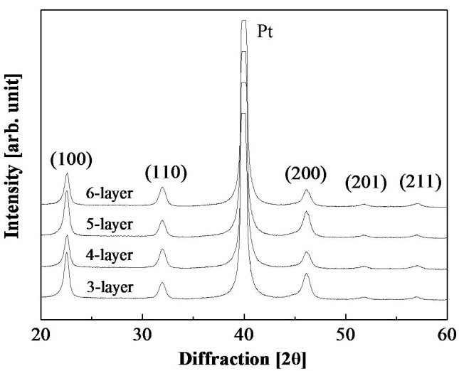
Figure 1 shows the X-ray diffraction patterns of the BFO/PZT heterolayered thin films. Generally, the crystallization behavior of the PZT films is substrate-dependent. For PZT films on Pt fired at a temperature lower than 700℃, with a Zr content of x>35, the pyrochlore phase (Pb2(Zr,Ti)2O6) was found [12]. These films were yellow in color. All of the films showed the typical XRD patterns of the perovskite polycrystalline structure, and the pyrochlore phase or preferred orientation was not observed. However, in the 3- and 5-layer thin films with the top layer of rhombic PZT(95/5) composition, the peak intensities of the (100) and (200) planes increased and the peaks of the (110) and (211) planes shifted to a high diffraction angle compared with those of the single PZT(95/5) thin film. The reason for this is assumed to be that the PZT films were more severely affected by the lower layer, because the Pb element was diffused into the Pt bottom electrode and the lower BFO layer during heating at 600℃.
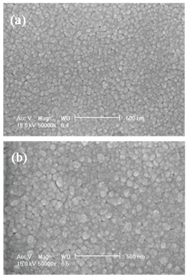
Figure 2 shows the surface SEM micrographs of the BFO/PZT films. The 5-layer film with the top layer of rhombic PZT(95/5) shown in Fig. 2 (a) shows a uniform and void free grain structure without the presence of the rosette structure. In general, the rosette structure can be found in sol-gel derived zirconium-rich PZT films [13], but it is not detected in the BFO/PZT heterolayered films. The reason for this is thought to be that the lower BFO films provide the nucleation site for the formation of the homogeneous perovskite phase in the upper PZT films [14]. The average grain sizes of the 5-layer and 6-layer films were about 60 nm and 80 nm, respectively.
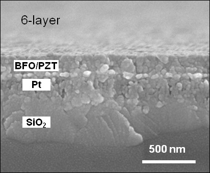
Figure 3 shows the cross-sectional SEM micrographs of the 6-layer BFO/PZT thin film. The thickness of the BFO/PZT films after one-cycle of drying/sintering is about 30-40 nm, and all of the films consist of a uniform grain with a relatively flat surface morphology. The Pt/SiO2 interfaces became very rough interfacial layers. This phenomenon can probably be explained by the fact that the diffusion of Pb from the PZT film into the Pt bottom electrode and the diffusion of Ti are severely advanced through the repeated annealing process. Also, the Pb diffusion becomes exacerbated by the higher concentrations of Zr in the PZT films [15].
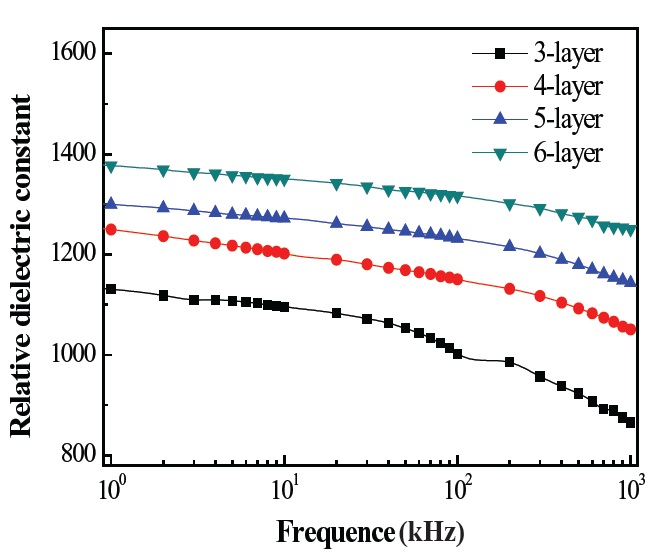
Figure 4 shows the relative dielectric constant of the BFO/PZT thin films as a function of the measuring frequency from 100 Hz to 1 MHz. The dielectric constant increases with an increase in the number of coatings and, an increase in the film thickness, and the 6-layer BFO/PZT film shows a good dielectric constant of 1360 at 1 KHz. BFO/PZT heterolayered thin films exhibit a superior dielectric constant compared with the single composition BFO (200 at 1 KHz) [16] and PZT(95/5) (358 at 100 KHz) [12] films. According to the report by J. Wang et al. [17], the crystal structure of rhombohedral BFO thin films fabricated on a SrRuO3 (SRO) electrode changed into the monoclinic crystal structure due to compressive stress imposed by the SRO electrode, which has an in-plane lattice parameter smaller than that of BFO. Also, the magnitude of the ionic displacements relative to the centrosymmetric strained perovskite structure was found to be extremely large. We consider that the rhombohedral crystal structure of the BFO films (a = 0.5634 nm) was distorted due to the large lattice mismatch and compressive stress imposed by the lower orthorhombic PZT film (a = 0.4149 nm, c = 0.4112 nm). Therefore, the BFO/PZT heterolayered thin films showed good dielectric properties due to the large ionic displacements in the distorted perovskite structure. With the frequency increase, the dielectric constant of the BFO/PZT thin films decreases linearly below 100 KHz and decreases quickly when the frequency is beyond 100 KHz. Generally, the dielectric dispersion results from the interfacial polarization, namely the Maxwell-Wagner relation caused by space charge polarization in the film/electrode and film/film interfaces [18]
In this paper, BFO/PZT hereolayered thin films, that were spin-coated on the Pt/Ti/SiO2/Si substrate, were prepared using the sol-gel method. The thickness of the BFO/PZT films after one cycle of drying/sintering is about 30-40 nm. All of the films showed a uniform grain structure without the presence of pyrochlore or a rosette structure. It can be assumed that the crystal growth of the upper BFO layers can be influenced by the lower PZT layers. The dielectric constant of the BFO/PZT heterolayered thin films were much better than those of the single composition BFO film and the PZT(95/5) film, and the dielectric constant of the 6-layer film was 1360 at 1 KHz. We consider that these properties of the BFO/PZT heterolayered thin films were caused by the distorted rhombohedral crystal structure of the BFO film due to the compressive stress imposed by the lower PZT film. The BFO/PZT heterolayered films showed a typical dielectric dispersion property, which indicated interfacial polarization caused by space charges in the film/film and film/electrode interfaces. However, further investigations and discussions are necessary to understand the interfacial characteristics and ferroelectric response in the BFO/PZT heterolayered thin films.