The decrease in the gate dimension has led to many new challenging barriers that need to be solved without a considerable trade off with the performance of other devices. Transistor Vth mismatch is one of the critical parameters to investigate [1,2]. An improvement of the mismatch with decreasing gate oxide thickness is well documented, as is the relationship between the mismatch and the layout area, that is, mismatch ∝ 1/(WL)1/2 [3].
The transistor Vth mismatch is more extreme in a transistor having a relatively thick gate oxide as implied by the abovementioned formula. Further, an n-type metal-oxidesemiconductor (n-MOS) transistor is known to be considerably weaker than a p-MOS transistor. The boron used for the Vth adjustment in an n-MOS transistor has a high diffusion rate because of the thermal budget. That is the reason why the n-MOS transistor with thick gate oxide has the worst Vth mismatch performance. Carbon prevents the boron from being diffused to the Si surface by trapping the interstitial Si through which the boron is diffused because of the thermal budget [4-6]. Carbon reacts with the interstitial Si according to the Watkins exchange mechanism [7], and then, the interstitial Si precipitates in the carbon-rich region. This carbon implant effect significantly reduces the thick n-MOS Vth mismatch in the 0.11-μm technology when it is used in the thick n-MOS Vth adjustment implant step. However, carbon induces an extremely abrupt electric field in a lightly doped drain (LDD) junction resulting in hot carrier injection (HCI) lifetime degradation [8]. This paper explains the HCI degradation mechanism in detail and suggests the use of a nitrogen implant in the LDD step to improve the HCI lifetime.
Further, a carbon implant is well known to deactivate the boron implanted in an n-type metal-oxide-semiconductor field-effect transistor (n-MOSFET) channel for Vth adjustment, resulting in a device performance shift [9]. This requires Vth implant tuning for a device performance match. The final process condition matching the device performance exhibits a perfectly flat Vth roll-off curve without the HCI issue in a thick n-MOS. Thus far, no research has reported this phenomenon. Hence, its detail mechanism is explained in this paper.
Carbon implants have been extensively investigated for Vth mismatch improvement. However, the side effects of the use of a carbon implant have not been investigated in detail [10]. This paper focuses on the unavoidable side effects on the transistor performance shift by the carbon implant, including their detail mechanisms. This paper suggests that the carbon implant should be combined with a critical process to prevent side effects. Finally, a number of characteristics of the carbon implant process are identified, and a clear process integration guideline for mass production is presented in this paper.
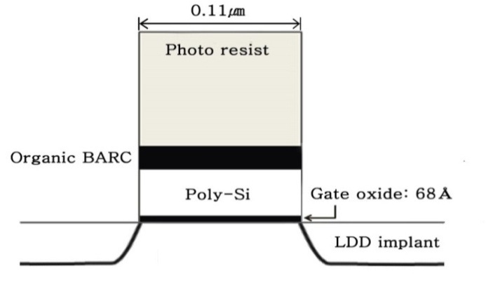
A (100)-oriented p-type wafer with a resistivity of 9?12 Ω-cm is cleaned using 1:19 diluted hydrogen fluoride, and a shallow trench isolation is formed. After well and threshold voltage (Vth) adjustment implantation, a carbon implant is added only in the thick n-MOSFET region (2.0 × 10¹⁴, 10 keV). The gate oxide is grown in a conventional furnace at 800℃ by using a wet oxidation process targeting 68 A and 20 A for the high- and low-voltage areas, respectively. Following the gate oxide growth, undoped polysilicon is deposited at 530℃ with 1,800 A. Photolithography for gate patterning is performed at a line width of 0.11 μm by using a 193-nm deep ultraviolet (DUV) lithography technology after the application of organic bottom anti-reflective coating (BARC; DUV32J, Brewer Science, Rolla, MO, USA) and photoresist (PR; SR540, Stanford Research System, Sunnyvale, CA, USA) coating targeting 750 A and 7600 A, respectively. A decoupled plasma source plasma etching reactor is used for BARC and the polysilicon gate etching process. Fig. 1 shows the detailed process schematic.
After gate poly formation, the LDD and the pocket implant are applied to the transistor. For a thick n-MOSFET, a nitrogen implant is added after the LDD implant with N2 (5.0 × 10¹⁴, 25 keV) to recover the HCI lifetime degradation caused by the carbon implant used in the Vth adjustment step.
A thick n-MOSFET is fabricated using the new process schematic and its electrical characteristics of the Vth mismatch, I?V curve, Isub curve, and Vth roll-off curve are determined using an Agilent HP4156 parameter analyzer.
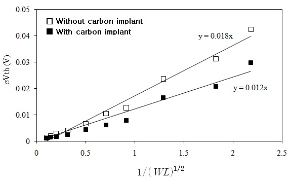
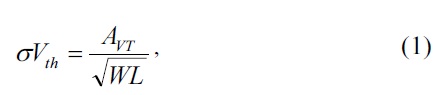
Theoretically, the MOSFET threshold voltage (Vth) variation and mismatch should be inversely proportional to the square root of the active transistor area as in (1) [3],
where
The carbon implant used in the Vth adjustment implant step significantly improves the Vth mismatch in a thick n-MOS of the 0.11-μm technology from 18 mV to 12 mV as shown in Fig. 2.
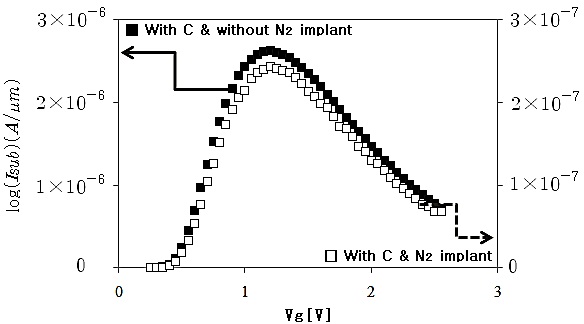
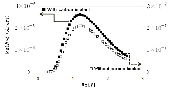
However, carbon induces an extremely abrupt electric field in the LDD junction by reducing the boron diffusion in the LDD junction [11], which cannot be simulated due to the tool limitation. This increases the substrate current (Isub) as shown in Fig. 3, resulting in HCI lifetime degradation. This degradation is due to the same mechanism as that of
the carbon-implant-induced Vth mismatch improvement by the prevention of boron diffusion in the channel region. The boron diffusion is suppressed in the LDD junction, causing an abrupt electric field profile in the LDD junction. The abrupt junction is known to increase the Isub, thereby degrading the HCI lifetime.
A nitrogen implant was applied in the LDD implant step to recover the graded junction from the abrupt junction caused by the carbon implant only in the LDD junction region without affecting the channel region. The nitrogen implant is known to improve the HCI lifetime by creating a graded electric field profile at the LDD junction. The inert
nitrogen leads to the formation of interstitial Si, helping the boron in the LDD junction to diffuse well and resulting in a graded junction. The nitrogen implant (5.0 × 10¹⁴, 25 keV) is proven to reduce the Isub to the level of the without carbon implant process as shown in Fig. 4.
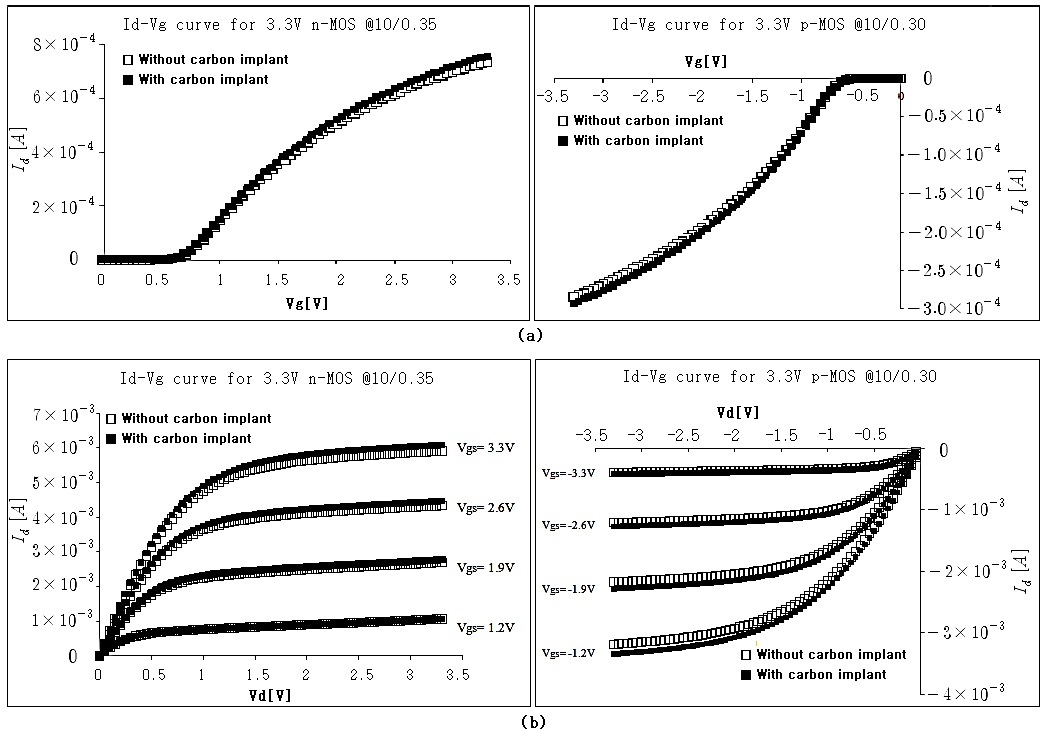
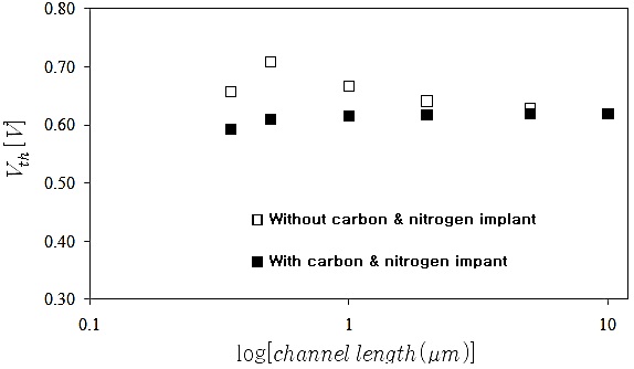
The carbon implant is known to deactivate the boron doped in the channel for the Vth adjustment, resulting in a Vth shift. Additional device tuning is carried out to recover this shift, as shown in Fig. 5.
The Vth curve verified using the new process schematic shows a perfectly flat curve that was never expected, as shown in Fig. 6.
Therefore, we need to understand the mechanism of the non-flat Vth roll-off curve for the case without the carbon implant in order to understand the estimated mechanism of the flat Vth curve in the case of with the carbon implant. The divot area, the boundary between the isolation oxide and the active area, is known to have a lower Vth than the channel Vth because the boron concentration in the divot area is lower than that in the channel. The lower Vth’ portion is large in the long channel; however, this portion decreases with a decrease in the channel length, resulting in a Vth increase. However, the Vth decreases again in a very short channel because of the short channel effect, resulting in a curve.
The carbon implant deactivates the boron as explained earlier, which is estimated to significantly reduce the Vth di-fference between the channel and the divot area. As a result, the contribution of the lower Vth in the divot area is the same as that along a different channel length, resulting in a perfectly flat Vth curve with respect to the channel length.
A carbon implant is investigated in detail from the perspectives of performance, advantages, and side effects for a thick (3.3-V) n-MOSFET. A carbon implant is very promising for transistor mismatching improvement with an ideal Vth roll-off curve. However, the carbon implant causes unavoidable side effects. This paper investigates critical issues, such as Isub increases and device performance shifts and suggests the use of a nitrogen implant and Vth fine-tuning as solutions. The new process integration schematic involving the addition of a nitrogen implant in the LDD process recovers the Isub degradation and the device performance shift caused by the carbon implant well. Finally, this study also investigated the Vth roll-off curve shift by the new process integration schematic and recommends this new schematic as a very promising process integration method with a perfect Vth roll-off curve device.