The improvement of device performance is a vital goal of the microelectronics community, and this can be done by scaling down the device dimensions [1]. However, as the technology scaling enters into the nanometer regime, the device exhibits various serious problems, such as low on current, increased leakage current, low reliability, and increase in manufacturing cost. To overcome these problems, various innovations in device structures have been researched and introduced. This has resulted in different structures with gate engineering, such as the Dual Material Gate (DM), Dual Insulator (DI) Gate, Gate Stack (GS), and channel engineering as graded channel (GC) [2,3]. Previously, Cheng et al. [4] have shown the impact of high-k gate dielectrics on the device short channel parameters. They have studied various short channel parameters, by taking gate stack engineering (i.e. one thick layer of high-k dielectric over one thin layer of low-k dielectric). Colinge [5] discussed the drive current and short channel effects (SCEs) for a SOI Multiple Gate MOSFET (MuGFET). From the simulation results, he concluded that SOI MuGFETs offer higher drive current, as well as better immunization to SCEs, than the conventional MOSFETs. Subramanian [6] presented a review paper on MuGFETs. He discussed the physics and technology of these devices, and their advantages and disadvantages. In Sharma et al. [3], different gate engineering and channel engineering under DG-MOSFET technology are discussed, and also a comparison of various parameters among DG-DM, DG-GC, DG-GS-DM and DG-GS-GC is highlighted. Aouaj et al. [7] and Bendib et al. [8] discussed the concept of GC and GS on the double gate platform. In this work, we presented three types of device structures, DG-FD, DG-GC and DG-DI, by keeping speed in mind, as well as power consumption. The important parameters, like sub threshold swing (SS), drain Induced Barrier Lowering (DIBL), on current (Ion), off current (Ioff), transconductance (gm), output conductance (gd) and Gain (gm/gd) are extracted, and a comparison is made among these three devices.
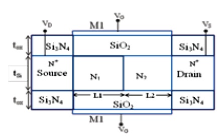
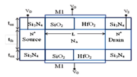
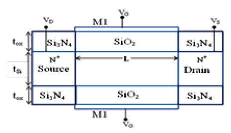
The schematic structures of DG-FD, DG-GC, and DG-DI MOSFETs are shown in Fig. 1. In all structures, the channel length (L) is fixed at 40 nm, as well as the Source/Drain length (LS/LD). The silicon thickness (tSi) is 10nm, and a uniform density of ND as 1020 cm-3 is considered. The channel is doped (NA) of 1018 cm-3 in DG-FD and DG-DI. Whereas for DG-GC, the high-low profile of doping is taken as 1018 cm-3 and 1017 cm-3. The oxide thickness tox = 2 nm, for all structurestructures a low-k spacer (Si3N4) is considered, for improvement of the device performance. The work function for the gate materials is assumed to be 4.8 ev.
To obtain accuracy of simulation, the mobility degradation that occurs inside inversion layers is accounted for. The degradation normally occurs as a result of higher surface scattering near the semiconductor-to-insulator interface. So in the simulation, the inversion-layer Lombardi constant voltage and temperature (CVT) mobility model is activated, which takes into account the effect of transverse fields, along with doping and temperature dependent parts of the mobility. These components are combined using Matthiessen’s rule, as follows:
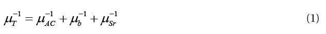
μAC is the surface mobility by scattering with acoustic phonons.
μSr is the surface roughness factor.
μb is the mobility by scattering with optical inter valley phonons.
The Shockley-Read-Hall (SRH) model simulates the leakage currents that exist due to thermal generation. Auger recombination models for minority carrier recombination have been used. In SOI technology, the potential in the channel is commonly referred to as “floating”. Furthermore, we chose Gummel’s method (or the decoupled method), which performs Gummel iteration for the Newton solution [9].
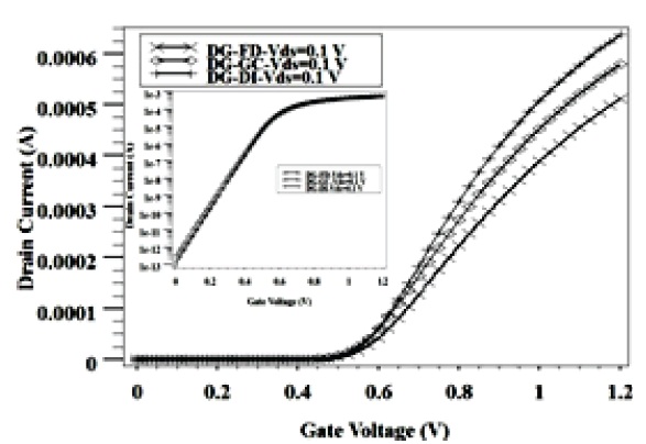
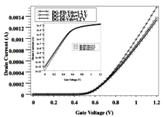
In Figs. 2 & 3, IDS-VGS transfer characteristics are shown on a linear scale and log scale (Inset Figures) for three different device structures, and are compared for VDS = 10 mV and 1.2 V. The DGDI MOSFET provides a larger drain current, as compared to the other two MOSFETs. This is because of the inclusion of higher dielectric material in the gate oxide, according to the relationship ID α Cox α εox.
The Sub threshold Slope (SS) is the major parameter for calculating the off state current. Furthermore, SS is calculated as:
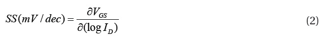
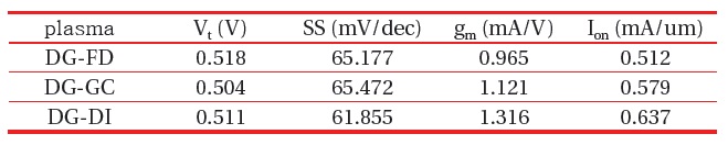
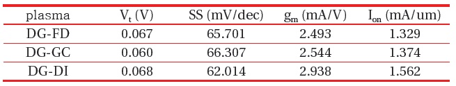
where, the logarithm is in base 10, ID is the drain current, and VGS is the gate voltage. The SS is always expressed in millivolts per decade. The typical value for the SS of Multigate MOSFET is 60 mV /decade, i.e. a 60 mV change in gate voltage brings about a tenfold change in drain current. The SS is extracted by calculating the inverse of maximum slope of VGS versus log (ID) curve, as shown in TABLE I. From the table, it is clear that the SS value is lower for DG-DI MOSFET, and again from equation (2)[10], the off state current is directly related to the SS. So, the off state current is also minimum for the DG-DI MOSFET, as compared to
the other MOSFETs, and as shown in Fig. 5.
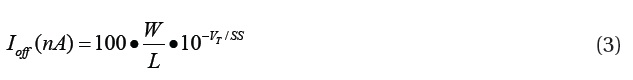
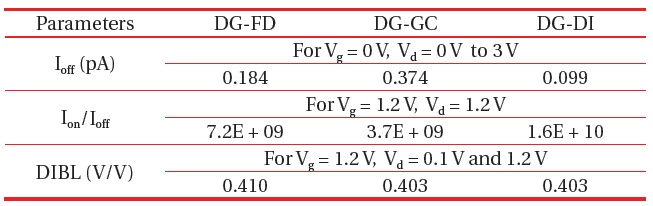
Again, the off state current (Ioff) is extracted, by calculating the drain current (ID) at VGS = 0 and VDS = VDD. The Ioff for all the three device structures is summarized in Table 3. It is important to keep Ioff very small, in order to minimize the static power dissipation when the device is in off state.
where, W : width of the channel, L : Channel Length, Q : Electronic Charge, VGS : Gate to Source Voltage, VT : Threshold Voltage, K: Boltzman Constant, T: Temperature in Kelvin, SS: Sub threshold Slope, and η : Body factor, which is proportional to the change in gate voltage with a change in channel potential, i.e.
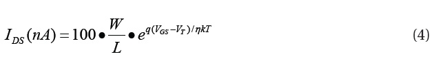
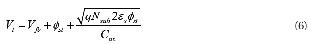
From equation (4)[10], the threshold voltage (Vth) is also a very important parameter for higher on state current, which improves the circuit speed. The Vth is extracted by calculating the maximum slope of the ID-VGS curve, finding the intercept with the xaxis, and then subtracting half of the applied drain bias, as given in Tables 1 and 2, for drain bias of 0.1 V & 1.2 V. The DG-GC shows a lower Vth, because of the high-low doping profile taken for the Graded Channel, and according to equation (6)[10], Vth is directly related to the doping profile. However, the doping profile being the same for DG-DI and DG-FD MOSFETs, the DG-DI MOSFET exhibits a lower Vth than DG-FD MOSFET, which enables its speed of operation.
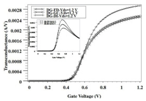
The gm versus VGS characteristics are compared for all the three device structures in Fig. 4. The DG-DI MOSFET shows a higher value of transconductance, when compared with the other two MOSFETs. As we know:
So, the value of gm is extracted by taking the derivative of the ID-VGS curve, the values of which are summarized in Table 1 and Table 2. From the extracted data, it can be examined that the DGDI MOSFET gives a higher gm value, and also a higher drain current. According to the relation in equation 7, gm is directly related to the drain current (ID). As far as analog circuits are concerned, gm is the most important parameter, because the value of gm is
[Table 1.] Extracted parameters at VD = 0.1 V.
Extracted parameters at VD = 0.1 V.
[Table 2.] Extracted parameters at VD = 1.2 V.
Extracted parameters at VD = 1.2 V.
directly related to the gain of the device (gm/gd).
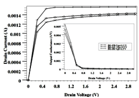
Figure 5 shows the output characteristics (IDS-VDS) and output conductance (inset figure) for various DG configurations, at a gate voltage of 1.2 V. The DG-DI MOSFET gives an almost flat characteristic in saturation, and also exhibits high drain current, in comparison with the other DG configurations. In order to demonstrate the SCEs, the simulated output conductance is given in the inset figure. In the saturation region, the DG-DI MOSFET exhibits the lowest value of gd, but it exhibits the highest value of gd in the linear region. The Ion/Ioff ratio and DIBL are given in Table 3 for all of the three device structures. The value of DIBL is calculated as per the relation given in equation 8.
The DIBL calculation is taken for Vth at VD = 0.1 V and VD = 1.2 V. Both DG-GC and DG-DI MOSFETs give nearly equal values of DIBL, which is better, as compared to the DG-FD MOSFET. This is because of the high-low doping profile in GC, and the inclusion of high-k dielectric material in the DI structure. The Ion/Ioff ratio is much higher for the DG-DI MOSFET than for the other two structures, which is a very important parameter for both speed and standby power consumption. For circuit speed application, Ion should be more, and for low power consumption application, Ioff should be less. So, there is always a tradeoff between Ioff and Ion.
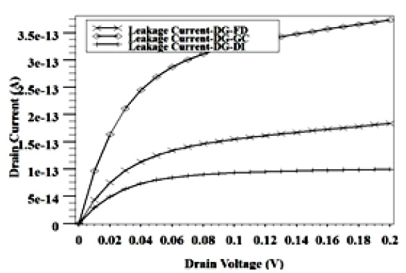
The leakage current (Ioff) is calculated by considering VGS = 0 for all the device structures, and is plotted in Fig. 6. It can be noticed that the DI architecture exhibits a very low leakage current, in comparison with the other two architectures. This is because the
physical thickness of the gate dielectric is more, due to the highk dielectric material used in the DI structure. On the other hand, from equation 3, Ioff is related in the ratio of Vt and SS. The DGDI architecture shows a higher value for the ratio of Vt and SS, as compared to the others, according to Table 1. Hence, it gives a lower Ioff, due to the exponential decaying nature of equation 3.
According to the International Technology Roadmap for Semiconductors, the SOI MOSFETs allow reduction of short channel effects. In order to study these new structures, numerical simulations are carried out. This work gives a close comparison of various design engineering, namely the FD, GC and DI of the DG-SOI. In this paper, the performance comparison for all the structures is limited to DC analysis only. Furthermore, the AC analysis can be done by investigating the analog and RF performance of the devices. The DG-DI MOSFET shows a significant
[Table 3.] Extracted and calculated parameters.
Extracted and calculated parameters.
improvement in device characteristics, such as on current (Ion), off current (Ioff), gm, SS and DIBL. Hence, DG-DI MOSFET is a suitable candidate for both high speed and low power consumption application. This paper verifies all the relations, through extractive data obtained from the simulation results.