Designing complex electronic systems to meet electromagnetic compatibility (EMC) requirements represents a significant challenge. The number of possible EM source/coupling- path/victim combinations in a system with hundreds of circuits can quickly become overwhelming. In addition, many of the configuration parameters, such as enclosure geometries, dielectric constants, and cable positions, may not be rigidly specified. For these reasons, the electromagnetic modeling tools that have revolutionized antenna and microwave system design have had relatively little impact on the EMC design of electronic systems. Effective EMC design requires a tool that can quickly evaluate very large numbers of source/coupling- path/victim combinations to identify those that are capable of causing a system to fail to meet its requirements. The tool must be able to produce meaningful results, even when some of the critical inputs are approximate or unspecified. Systematically evaluating and approving every possible source/coupling-path/victim combination in a complex electronic system is the fundamental premise of a
Antenna and microwave systems are generally designed with very specific performance objectives. For example, an antenna might be required to have a gain specified to within 1 dB over a given bandwidth. That design objective would play a major role in the design and development of the antenna, and with the help of full-wave numerical electromagnetic modeling tools, the first prototype would be likely to meet that objective.
Digital electronic devices also have specific performance objectives when it comes to unintentional electromagnetic emissions. These devices have to comply with maximum radiated emissions requirements such as those described in CISPR 22 [1] or the US Federal Communications Commission (FCC) Rules and Regulations [2]. However, unlike antenna and microwave systems, electronic device design decisions at the board level are rarely made based on specific design objectives. Since unintentional radiated emissions are generally undesirable, the goal of the design is usually to minimize them. And since the radiated emissions depend on a large number of variables, including many that are unknown or uncontrolled by the designer, it is often impossible to predict the specific effect that any particular design decision will ultimately have on a radiated emissions test.
As a result, full-wave field solvers are not very good at predicting unintentional radiated emissions. Numerical field solvers give precise solutions to precisely framed problems. They are not well suited for solving complex problems where specific details (e.g., cable positions, dielectric constants, source impedances, etc.) are not precisely specified.
Without simulation tools, circuit board designers are generally forced to rely on experience with other products and EMC design guidelines or rules-of-thumb to make design decisions, e.g., [3-6]. While EMC design rules can be helpful, they cannot guarantee that the device will ultimately meet its requirements. Furthermore, the indiscriminate application of design rules is likely to result in a design that is more complex and costly than necessary.
In 1995, researchers at the University of Missouri-Rolla (UMR, now Missouri S&T) teamed up with engineers at Quad Design, Sun Microsystems, and other electronics companies to develop a software tool that would help product designers meet EMC requirements. They formed the
Ultimately, the software development did not keep up with the algorithm development and several user interface issues were never resolved. As a result, there is currently no commercial software that fulfills the original vision of the EMI expert system. Nevertheless, the insight and closedform equations developed over the years can be readily applied to most circuit board designs. Since the algorithms calculate the maximum possible radiated emissions that can occur due to various sources and structures on a circuit board, it is possible to systematically design boards that are guaranteed to meet specific EMC requirements. The following sections describe this procedure and apply it to an example design.
Ⅱ. PERFORMANCE-BASED EMC DESIGN
The goal of performance-based EMC design is to ensure that each component and circuit on a printed circuit board is incapable of causing the device to fail to meet its EMC requirements [24]. To accomplish this, the maximum radiated emissions originating from the component/circuit are calculated for all possible coupling-path-antenna structures, with all unknown variables (e.g., dielectric constants, cable lengths, etc.) set to their worst-case values. This approach requires that the design be reviewed circuit-by-circuit to ensure that the electrical and geometric parameters associated with any circuit will not allow sufficient energy (in or out) to cause an EMC failure under any circumstances.
1. Start with the EMC Requirement
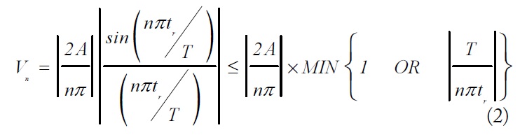
The first step in the process of performance-based EMC design is to identify the requirements. For example, CISPR 22 requires that the radiated field strength 10 m from a product be no greater than 30 dB(μV/m) or 31.6 μV/m at 100MHz. This means that the power radiated must satisfy:
where
2. Control the Signal Bandwidths
One relatively easy way to limit the unnecessary power in a signal or circuit is to limit the bandwidth to those frequencies necessary for the proper operation of the device. For analog circuits, this is usually done by filtering. For baseband digital circuits, this usually means controlling the signal transition times.
Any digital circuit source that cannot deliver at least 1 nW of power at 100MHz cannot be the sole source of radiated emissions that exceed the specification in the example above. This is true no matter how poorly the circuit is routed and no matter what other circuits or structures the signal may couple to. A primary objective in performance-based EMC design is to ensure that no source produces power capable of exceeding the specification unless that power is necessary for the circuit to serve its intended function.
For every digital circuit in the system that is operating at clock speeds of 20MHz or less, the best way to control the emissions at 100MHz and higher is to control the transition times. Slowing transition times to 20% of the bit width significantly reduces the energy in the signal at frequencies above the fifth harmonic. For example, suppose our signal source is a clock output with a 2.5-volt signal amplitude and a 50-Ω source resistance (i.e., 50 mA max current). If the operating frequency is 1MHz and we’re driving a 5-pF load, the bit width is 1 μs and the transition time is approximately 0.55 ns (2.2RC). The signal voltage at each odd nth harmonic of the clock frequency (assuming a trapezoidal waveform) is given by:
where
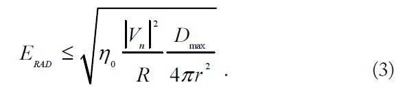
Fig. 1 shows a plot of the maximum possible radiated emissions compared to an FCC Class B radiated emissions test limit. Note that this component is capable of producing radiated emissions about 30 dB above the limit at 100MHz.
Now suppose we insert a 20-kΩ resistor in series with the output of this controller. For the same 5-pF load, the transition time increases to 220 ns. Since the transition time is about 22% of the bit width, the integrity of the digital signal is preserved. Fig. 2 shows the radiated emissions that would result if all of the power produced by this source was radiated. Note that this circuit is incapable of producing enough power to exceed the FCC Class B radiated emission specification at any frequency above 90MHz. From a design standpoint, this means that no matter how poorly the routing is done, or how many other circuits this signal couples to, it cannot be the source of a radiated emission failure at frequencies above 90MHz.
Controlling the transition times is an important step in the process of guaranteeing compliance with a radiated emission specification, because it puts an upper bound on the frequencies that must be considered when evaluating possible source/coupling-path/antenna combinations. Higher frequencies have shorter wavelengths and can be radiated efficiently by smaller structures. Putting an upper bound on the frequencies that need to be considered reduces the number of possible radiating structures on the board. Low upper bounds make it easier to identify troublesome features of the design and eliminate them.
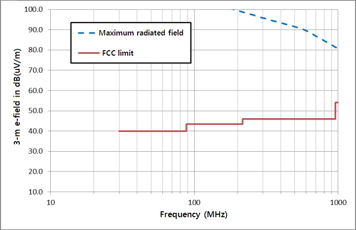
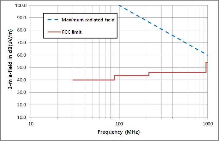
Faster digital circuits will have higher upper bounds on the frequencies that need to be considered, but controlling transition times reduces the amount of power available to be radiated even at frequencies below the upper bound. Series resistors are one way to control transition times. The use of controlled slew-rate sources can also be effective. Fig. 3 shows the maximum possible radiated emissions from the same clock in the previous example when it is operating at 32 MHz. Note that it is capable of exceeding the limit by about 50 dB at 96MHz (the third harmonic); and is not guaranteed to meet the requirement at any frequency below 1 GHz. Slowing the transition time down to 6.0 ns using a 500-Ω resistor results in the maximum emissions plotted in Fig. 4. Although the circuit is still not guaranteed to meet the specification at any frequency below 1 GHz, the power available at the higher frequencies is significantly reduced.
3. Control Current Paths and Coupling
Controlling all transition times significantly reduces the number of circuits capable of contributing to a radiated emissions problem in a typical electronic system. It should be noted that circuits capable of radiating a few dB above the limit are unlikely to do so. The calculations in the previous section assume that the source is connected to a lossless impedance-matched antenna. This is unlikely to happen in a real device, so the actual emissions will generally be lower than the maximum possible emissions. Nevertheless, each circuit capable of radiating above the specification limit should be examined to ensure that most of the power being supplied at the offending frequencies reaches the load. The best way to do this is to trace the signal current paths from the source to the load and back again.
During the design review, it is important to recognize any structures or coupling paths that could steal power from the intended signal path and direct it elsewhere. Traces over a solid ground plane (microstrip traces) are relatively easy to examine, because they present fewer opportunities for unwanted coupling. Levels of crosstalk between adjacent microstrip traces can easily be kept below 20 dB simply by following general design guidelines for trace routing. If your maximum coupling is 20 dB, then the maximum radiated power will be 20 dB lower than the maximum available power calculated in the previous section.
4. Evaluate Radiation Mechanisms
In order to guarantee compliance with the radiated emissions requirements, every circuit in the entire system must be examined and all possible radiation mechanisms must be evaluated. A radiation mechanism is a means by which power in a signal that is not dissipated in the load, can be converted into radiated power. Possible radiation mechanisms include:
1) Differential-mode radiation where the signal path itself acts as an antenna and radiates some of the signal;
2) Coupling from the signal path to other structures on the board that act as antennas (e.g., large heatsinks or power planes);
3) Coupling of the signal that induces common-mode currents on attached cables or the enclosure.
In practical systems, the process of controlling transition times and tracing current paths can eliminate a large number of circuits from further consideration. The remaining circuits can be evaluated using the maximum radiated emissions algorithms that were developed for the EMI expert system [9-23]. Several of these are implemented in a web-based calculator Laboratory website [25]. Maximum emissions calculations basically assume that everything not known about a particular source/ antenna geometry is worst-case. For example, if a source drives a cable of unknown length, the calculator assumes that the cable is a lossless, resonant antenna at every frequency of interest. If a transition time is unknown, it is assumed to be zero. While these calculations will generally overestimate the actual measured radiated emissions, they do provide an upper bound. For EMC work, an upper bound is generally preferable to an exact calculation of emissions from a specific configuration. Designing a system to be compliant with a radiated emissions specification based on maximum emissions calculations, ensures that the specification will be met regardless of where the system is tested, or what it is connected to.
Suppose the 32-MHz clock circuit described in the previous section is implemented on a printed circuit board. It propagates down a 10-cm microstrip trace located 1 mm above a solid plane that returns the current to its source. The transition time has been slowed to 6.0 ns using a 500- Ω series resistor. As indicated in Fig. 4, there is enough power in this signal to present a radiated emissions problem at harmonics up to and exceeding 1 GHz, so the circuit can’t be ignored. The maximum possible emissions from this circuit must be evaluated for each possible radiation mechanism.
1. Differential-Mode Radiation
Direct radiation of a signal by the conductors that form the signal path is known as differential-mode radiation. It basically occurs because the fields developed by currents flowing in one direction (e.g., source-to-load) are not exactly canceled by the fields developed by the return currents flowing in the opposite direction. A basic formula for the radiated field from two parallel wire segments carrying a differential-mode current, Id, is given by [26],
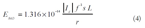
where
Note that the maximum possible emissions from this trace are approximately 30 dB below the FCC Class B radiated emission limit, which is 40 dB (μV/m) at 32MHz. Differential- mode radiation from signals on traces routed above a ground plane is rarely significant. For this reason, calculation of the differential-mode radiated emissions is usually unnecessary for any reasonable routing of high-speed signals.
2. Direct Coupling of the Signal to I/O Traces
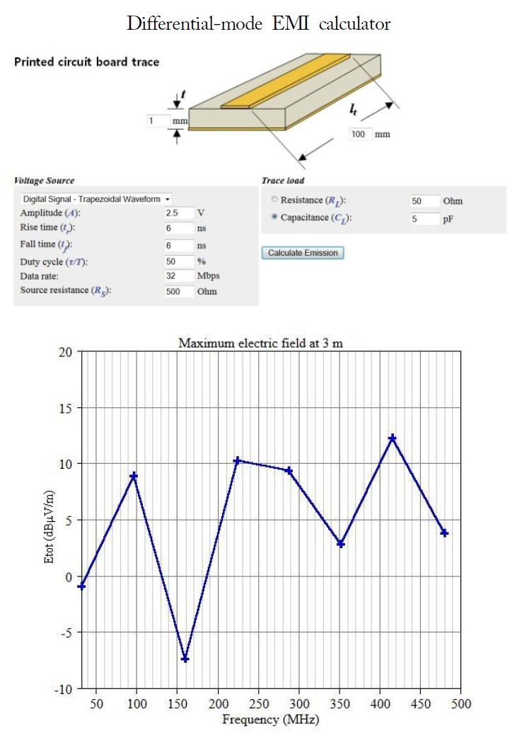
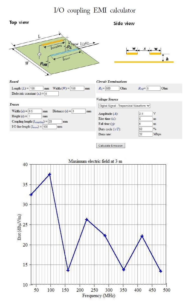
The cables attached to a board generally represent some of the best possible “antennas” in an electronic system. One way that signal power on traces can be converted to radiated emissions is when fields from the signal trace induce crosstalk on a nearby trace that connects directly to the attached cables. This radiation mechanism was examined extensively in [22] and the algorithms developed were incorporated in the MREMC calculator [27]. Fig. 6 shows the results of this algorithm applied to the 32-MHz clock trace when a 20- mm section of the clock trace is located 3 mm away from an I/O trace. In this calculation, the board size is 15 cm × 15 cm and the dielectric has a relative permittivity of 4. Note that in this example, the maximum possible emissions due to this radiation mechanism are still below the FCC Class B limit indicating that the separation is sufficient.
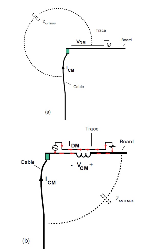
3. Common-mode Currents Induced on Cables Attached to the Board
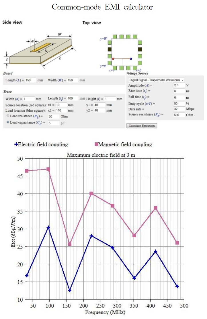
Another possible radiation mechanism is electric or magnetic field coupling from the clock trace that induces common- mode currents on attached cables without coupling to an I/O trace. This is one of the most common reasons that some systems fail to meet radiated emissions requirements. Common-mode currents as low as 5 ×A induced on a 1-m cable can result in radiated fields that exceed the FCC Class B limit. The physics of this coupling was first described and quantified in [9,10], and refinements to the original model have been developed over the years [14,16,17,19,21]. Electric-field (or voltage-driven) coupling is illustrated in Fig. 7(a). The difference in the electric potential of the trace relative to the cable is ultimately responsible for the development of the common-mode currents on the cable. Magnetic-field (or current-driven) coupling is the result of a mutual inductance between the signal current path and the effective antenna formed by the board and its attached cables, as illustrated in Fig. 7(b). Equations for determining the amplitude of an equivalent common-mode voltage source that drives the cable are derived in [14,19]. Equations for deriving the maximum possible radiated emissions from a board-cable structure driven by a common-mode voltage source are derived and validated in [17,21].
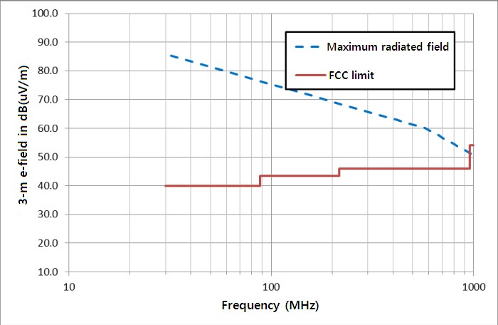
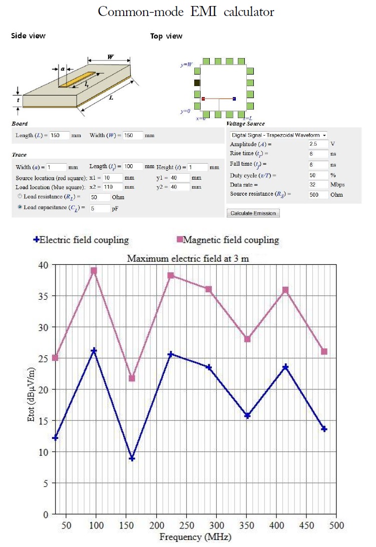
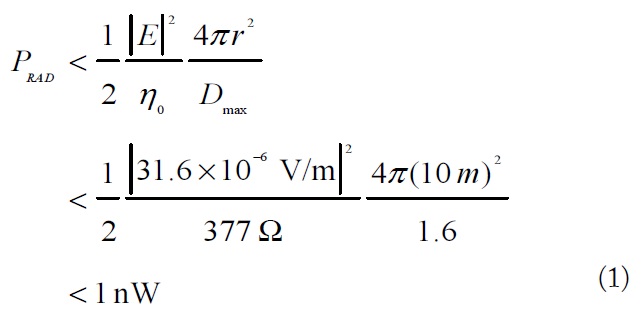
The algorithms implementing the equations derived in [19,21] were incorporated in the MREMC calculator. Fig. 8 shows the results of these algorithms applied to the 32MHz clock trace when it is 10 cm long on a board that is 15 cm×15 cm. In this case the board has one attached cable. The position of the attached cable is indicated by the black square in the “ Top view” section of the figure.
The trace location is indicated by the red line. Note that the maximum possible field radiated due to the electric-field coupling mechanism is more than 20 dB below the limit at all frequencies. The maximum possible field radiated due to the magnetic-field coupling mechanism is also less than the FCC Class B limit, approximately 40 dB(μV/m), although it is very close at some frequencies.
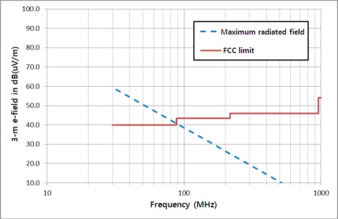
Fig. 9 shows the results of the same calculations for the same board with two cable attachment points. In this configuration, the maximum possible radiated emissions exceed the FCC Class B limit at frequencies below about 120MHz. If it were absolutely necessary to locate this trace between the two connectors, it would be necessary to reduce the height or length of the trace, or bury the trace between planes in the layer stack-up, in order to guarantee compliance with the FCC Class B specification. The calculator allows a designer to experiment with various options until a design that is guaranteed to comply with the requirements is found.
The design example above illustrates how one trace would be evaluated using the performance-based design methodology. A similar evaluation would be performed on every circuit board trace evaluating all potential radiation mechanisms. With this methodology, designers make decisions based on the EMC requirements, rather than attempting to comply with design rules that may or may not be relevant in a given situation.
Manually examining and evaluating every circuit on a board that may have hundreds of circuits might seem like an overwhelming task. However with a little experience, a designer can learn to recognize many of the circuits that are incapable of being the source of a problem without explicitly doing a calculation. Also, simple changes that convert possible sources to negligible contributors will become evident to the designer over time. This will make it easier to simply adjust the design rather than explicitly evaluate the maximum emissions due to all possible radiation mechanisms. Since many of the calculations required for this procedure can be automated, these calculations can eventually be integrated with existing computer-aided design tools. This will further reduce the burden on the design engineer, and reduce the level of EMC design experience required to implement the procedure.
There are many advantages to a performance-based EMC design approach. Although the technique requires more time and effort than a design-rule based approach, it is much more likely to result in a low-cost, compliant design on the first pass. The performance-based EMC design approach also highlights the most vulnerable aspects of a design, making it easier to diagnose any problems that may occur in the field.
On the other hand, the rigorous, but arbitrary enforcement of EMC design rules can add cost and complexity to a design without necessarily improving its EMC performance. In fact, the misapplication of a well-intended design rule can significantly degrade EMC performance [3].
Finally, one might expect that designing for guaranteed compliance would result in products that are over-designed and expensive. However, most of the EMC design decisions made early in a product’s development cycle have little or no impact on the cost of the product. The costs associated with building a compliant product based on the procedure outlined above are generally a tiny fraction of the product cost. On the other hand, the costs associated with fixing an EMC problem in a product that has already been prototyped can be relatively high.
The procedure described in this paper focuses on meeting radiated emissions requirements. A similar approach could be used to guarantee compliance with conducted emissions and susceptibility requirements.