

Microelectromechanical Systems (MEMS) switches [1] optimized to work at Radio Frequencies (RF) have been a primary focus of intensive research over the past few years in both academia and industrial organizations. RF MEMS switches have grown at very fast pace, and have entered into many applications in wireless communication [2] and space systems. RF MEMS switches have replaced the conventional GaAs FET and p-i-n diode switches in RF and microwave systems, because of their negligible power consumption of a few μ-watts, low insertion loss, high isolation, much lower intermodulation distortion, small footprints, low cost, and light weight [3]. Due to the enormous advantages of MEMS switches, these are widely used at RF to millimeter-wave frequencies.
Typically MEMS switches are fabricated using surface micromachining processes, and have a suspended thin metal membrane called the “bridge,” which can be a fixed-fixed, cantilever, or torsion beam). The bridge allows or blocks the electronic transmission through mechanical movement of the membrane above the electrode [3]. MEMS switches can be actuated by various methods, such as electrostatic [4-6], electromagnetic [7], piezoelectric [8], and thermal [9] actuation. Due to the near-zero power consumption and linearity, electrostatic actuation is most widely used, in which electrostatic force is generated between a fixed electrode and a movable membrane for switching operation. Several disadvantages include slow switching speeds, high actuation voltage, and hot switching in high-power RF applications [10].
This paper presents a novel design for a RF MEMS capacitive switch on quartz substrate, which results in excellent RF performance in the k-band with high isolation and low insertion loss. With the inclusion of ribs around the membrane, the bucking effect and stiction problem can be eliminated. The effect of this novel membrane design can be seen in stress analysis. The membrane can withstand several switching cycles. The spring constant, required voltage, and stress is analyzed using multiphysics environment.
2.1 Structure and principle of operation
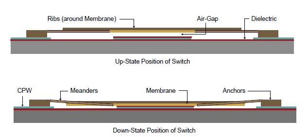
The proposed RF MEMS switch has a coplanar waveguide (CPW) line for RF signal transmission on a 100-μm-thick quartz substrate. A dielectric layer of hafnium dioxide (HfO2) is used due to its very high dielectric constant over the substrate. The working principle of the switch is shown in Fig. 1. The CPW consists of a 70-μm-wide signal line with a gap of 90 μm. The same dielectric material is used on top of the signal line. The characteristics of the switch are mainly governed by the design of the membrane.
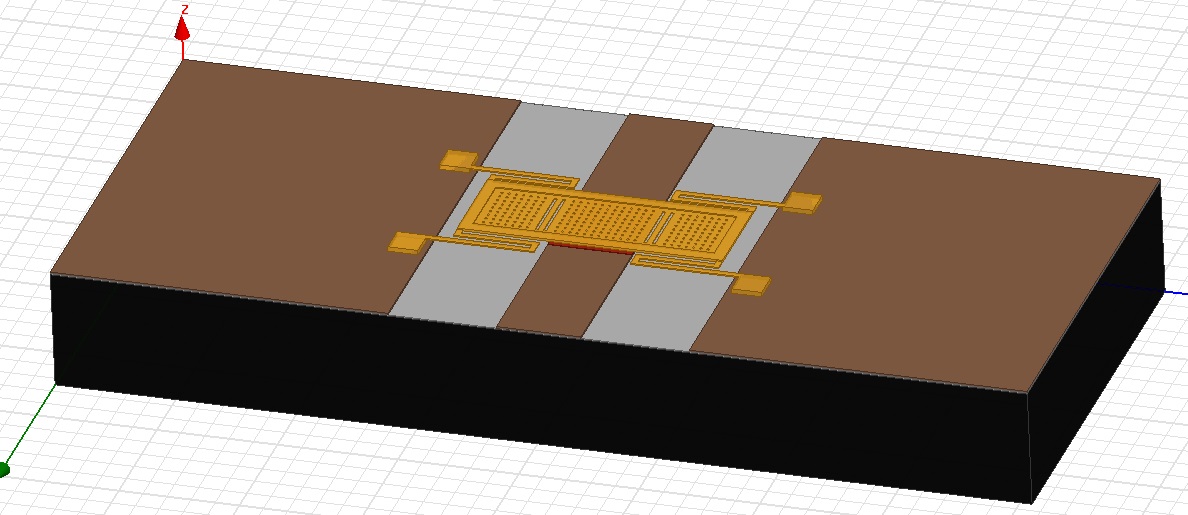
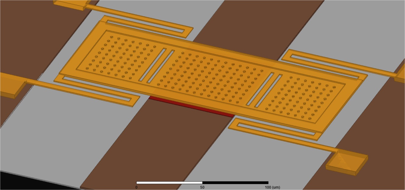
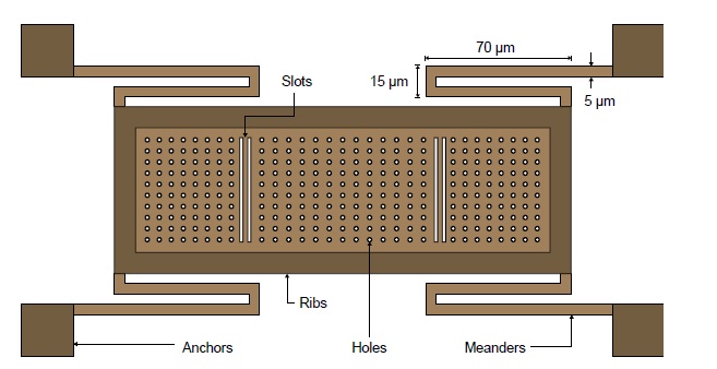
To lower the pull-down voltage, meanders are included on the sides of the membrane, which helps to lower the spring constant of the membrane. The membrane is thin on the inside and thick at its boundary. Four anchors 4-μm thick are attached to the ground plane, and meanders are present on the top end to give the membrane a proper space for movement above the RF line. A gap height g0 of 3 μm is maintained between the membrane and pull-down electrode, as it is needed to optimize the pull-down voltage and gap. Otherwise, the membrane may become prone to self-biasing and external vibrations, and then it would not be possible to recover the membrane’s position due to elastic recovery forces. A 3D view of the proposed switch is shown in Fig. 2, and a tilted view of the switch membrane is shown in Fig. 3, showing the varying height of membrane.
The proposed switch is actuated by electrostatic force. When a voltage is applied to the pull-down electrode, the membrane connected to the grounds of the CPW line snaps down onto the signal line. As the dielectric layer is applied to the signal line, it reduces the gap g0, and the down-state capacitance value is increased. When the membrane is in the up-state, the capacitance value becomes low, thus giving a good capacitance ratio. The design is optimized after the analysis of the von Mises stress and spring constant constraints.
The inclusion of holes of 5-μm diameter and slots in the membrane help to reduce the biaxial residual stress, and thus reduce the buckling effect of the membrane after the removal of the sacrificial layer during fabrication. The membrane is reliable in terms of switching life due to the flatbed internal structure. Hence, the membrane does not bend when pulled in towards the signal line. The bending only occurs at the meanders. The holes also help in reducing the principle strain on the membrane at the pull down electrode area. The diameter of the holes in the membrane should be less than 2g0, so as not to affect the capacitance value. In MEMS switches, if the spring constant
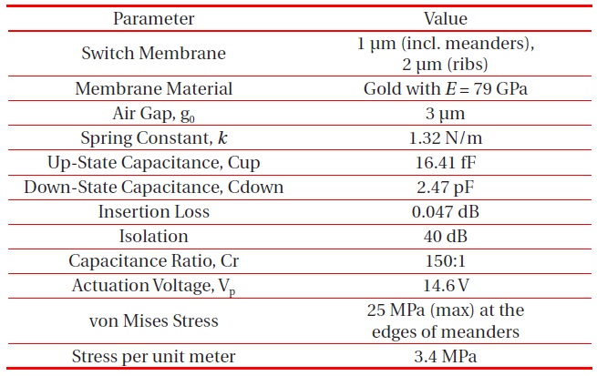
The proposed shunt switch is designed in Ansoft HFSS v13, which was also used to measure the RF performance. A combined multiphysics environment, COMSOL Multiphysics 4.3b, is used to compute stress, the required actuation voltage, and the spring constant. The specifications, dimensions, and materials used to design the switch are presented in Table 1.
A flat and smooth substrate surface is preferred to fabricate the switch, as the substrate is the base over which the switch operates. It should have uniform electrical properties and
[Table 1.] Switch specifications.
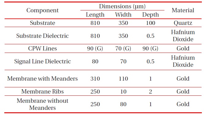
Switch specifications.
chemical resistance (as required during fabrication) [11,16]. These requirements make quartz a good candidate, as it fulfills all these requirements. Quartz has a high melting point compared to silicon, so a switch designed with a quartz substrate can withstand higher temperatures than one made with a silicon substrate [3].
Hafnium dioxide (HfO2) of 0.5-μm thickness is used over the substrate beneath a CPW line made of Gold (Au). HfO2 has a dielectric constant of k~25. It is always preferable to use materials that have high k [12]. Most of the conventionally designed MEMS switches have used silicon dioxide (SiO2) or silicon nitride (Si3N4) as dielectric materials, with k~3.9 and k~7.5, respectively. As the research evolved, more advanced materials came into existence. We compared these materials with the one actually used in the switch, and the results indicate that HfO2 provides higher isolation compared to other dielectric materials.
2.5.1 Actuation mechanics and power handling capabilities
Due to the approach used to design the membrane, the load on the membrane is shifted toward the ends, and it has meanders to lower the overall spring constant
The actuation voltage
where
The analytical value of the actuation voltage is 14.6 V for the dimensions of the switch given in Table 1. The permittivity
The power handling capability is augmented in comparison to various designs due to the use of a single electrode. The switch relies on the elastic recovery force of the meanders instead of the force of the membrane to pull it upwards, because the membrane is stiff around edges.
2.6 Electromagnetic circuit modeling
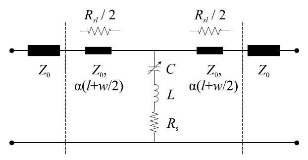
A lumped CLR model [13,14] of the membrane and two sections of the transmission line are used to model the capacitive switch with a capacitance having the down-state/up-state values. Figure 5 shows the equivalent circuit model of the switch. The sections of the transmission line are of length
The shunt impedance of the switch is given by:
with
The CLR model behaves purely as a capacitor for frequencies below the
When the resonant frequency is 555 GHz, the inductance of the membrane plays absolutely no role in the up-state for
It is preferred to use the down-state resonant frequency (
Silicon is used for the membrane, as it is robust and has a low initial stress for bending compared to Au or Al membranes. Hence, it has no residual stress component, which results in locally different bending of the membrane, and a constant gap is maintained between the membrane and transmission line. The various parameters of the silicon material used in the membrane design are given in Table 2.
The parallel plate capacitance of a shunt switch is given calculated as:
The dielectric constant
0.5-μm thickness is used with a gap height
2.6.2 Down-state capacitance
The down-state capacitance of the switch is calculated for when the membrane is in the down position. The calculated value of the down-state capacitance is 2.47 pF. In the down position, the thickness of the dielectric layer is so small that the fringing capacitance can be neglected. The down-state capacitance can be calculated by:
2.6.3 Capacitance ratio
The preferred value of the capacitance ratio should be greater than 100:1 [3]. In the calculation of the capacitance ratio, the result is 150:1 with an up-state capacitance of
By varying the thickness of the dielectric layer to improve the capacitance ratio, the optimized thickness of the dielectric is used, as we cannot go beyond one particular value. The RF MEMS switch needs an actuation voltage, and if the dielectric layer is very thin, it can cause dielectric breakdown.
2.6.4 Series resistance and inductance
The main factors for the calculation of series resistance are
To model the inductance in the down-state position of the switch, it is assumed that the capacitance is large enough for it to act as a short circuit. The short circuit model can be analyzed numerically or by using an electromagnetic tool like Ansoft HFSS. The inductance in the down-state is given as:
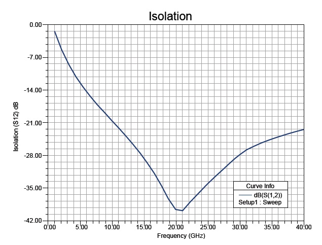
The isolation loss, return loss, and insertion loss of the proposed switch are measured using Ansoft HFSS v13. The RF performance of the switch is observed between frequencies of 1 GHz and 40 GHz. From Fig. 6, it is clear that the switch gives an excellent isolation S12 of -40 dB at 21 GHz in the down-state.
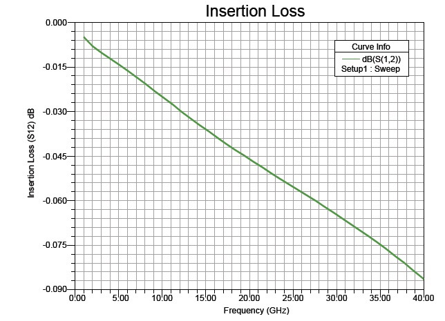
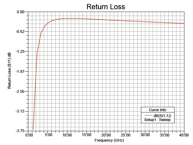
Table 2 manifests the switch performance for the k-band.For the up-state position, the insertion loss S12 is analyzed, and the results in Fig. 7 show a low insertion loss of -0.047 dB in the upstate. The return loss S11 is calculated, and Fig. 8 presents a plot of the return loss. The results show that the switch has excellent performance in the k-band.
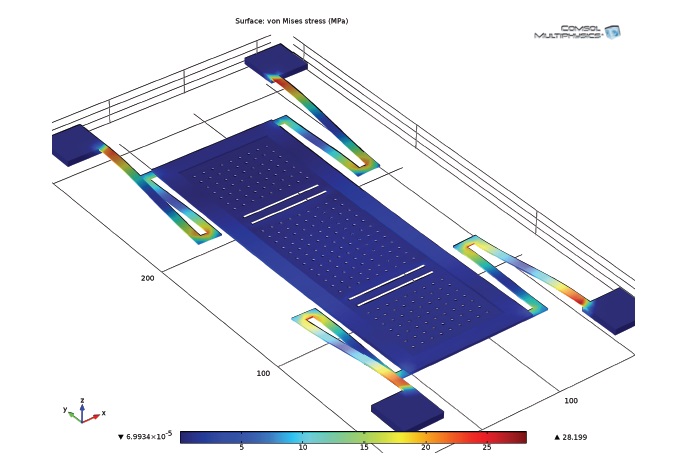
The von Mises Stress is analyzed to check the deflection of the membrane due to stress for the desired height. The membrane is made of gold, which has a maximum stress of 25 MPa. This value is good enough to handle higher switching under the given maximum stress. Figure 9 shows the deflection of the membrane under stress.
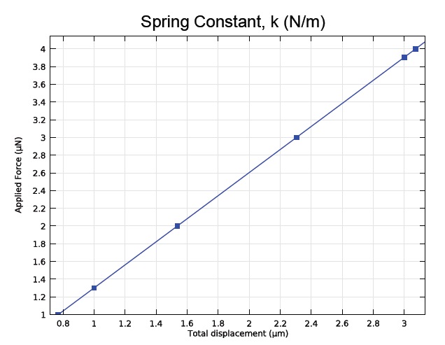
The spring constant
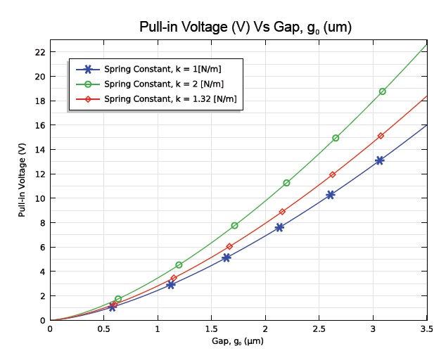
The pull-in voltage or the electrostatic actuation voltage required to pull the membrane down to change the state of the switch can be calculated by eq. (1). The pull-in voltage is plotted vs. the gap in between the membrane and the signal line in Fig. 11. The graph is plotted for the spring constants k = 1, 2, and 1.32 (N/m). It is clear from the plot that as the gap and spring constant increase, higher pull-in voltages are required for switching actions. Hence, the design is optimized to work at 14.6 V for a 3-μm gap height with low
The proposed design utilizes a novel approach of membrane design, as the membrane is a hybrid in terms of thickness, and it
is designed to reduce the buckling effect and to reduce the overall spring constant. From the numerical calculations and simulations, it is clear that the switch shows excellent isolation and insertion loss in the k-band. The meanders and ribs are designed so that the stiction problem in the switch can be reduced, and holes and slots in the membrane reduce the fringing fields and air resistance under the membrane, allowing the switching speed to be increased. The reliability of the switch can be approximated
by the von Mises stress analysis.
The switch operates at lower actuation voltage than other capacitive switches. This results in excellent RF response, which allows the switch to be used in applications where low power and low loss are a primary concerns, such as in wireless communication and space systems.
[Table 2.] Performance analysis.
Performance analysis.
