We investigated the etching characteristics of TaN thin films in an O2/BCl3/Cl2/Ar gas using a high density plasma (HDP) system. A maximum etch rate of the TaN thin films and the selectivity of TaN to SiO2 were obtained as 172.7 nm/min and 6.27 in the O2/BCl3/Cl2/Ar (3:2:18:10 sccm) gas mixture, respectively. At the same time, the etch rate was measured as a function of the etching parameters, such as the RF power, DC-bias voltage, and process pressure. The chemical states on the surface of the etched TaN thin films were investigated using X-ray photoelectron spectroscopy. Auger electron spectroscopy was used for elemental analysis on the surface of the etched TaN thin films. These surface analyses confirm that the surface of the etched TaN thin film is formed with the nonvolatile by-product.
As the critical dimensions of the metal-oxide semiconductor field-effect transistor shrank for the 45 nm node and those below, the scaling down of SiO2 thickness has exacerbated the problems such as increased leakage current, poly-Si gate depletion, and boron penetration into the channel region [1,2]. To overcome these problems, the conventional poly-Si gates on ultrathin SiO2 dielectric layers could be replaced by metal gates on high-
In this work, we investigated the etch characteristics of TaN thin films using an inductively coupled plasma (ICP) system. The etching characteristics of the TaN thin film were investigated in terms of the selectivity of TaN to SiO2 as a function of Cl-based gas chemistry. The chemical states on the surface of the etched TaN thin film were investigated by X-ray photoelectron spectroscopy (XPS). Auger electron spectroscopy (AES) was used for the elemental analysis on the surfaces of the etched TaN thin film.
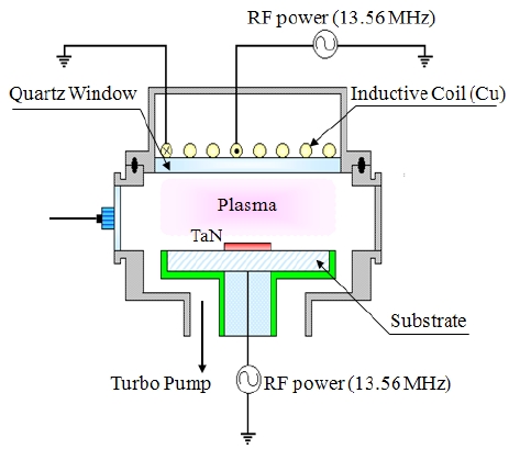
The TaN thin films were deposited on SiO2/Si 6-in p-type (100) wafers by the atomic layer deposition (ALD) system. Before the deposition of the TaN thin films, pre-cleaning and oxidation processes for the Si wafer were required to obtain good thermal interface compatibility with the TaN thin film, which was deposited on the SiO2(100 nm)/Si(100) by ALD with a thickness of 100 nm. The dry etching of the TaN thin films was performed using an ICP system [14]. A 13.56 MHz power generator was connected to a 3.5 turn copper coil to generate the ICP. Another 13.56 MHz power
generator was attached to the substrate electrode to control the DC-bias voltage. The substrate temperature was kept at 40℃ with a water cooling system. The chamber was pumped to 10-4 Pa. The final pressure was lower than 10-4 Pa with a turbo-molecular pump. The etching characteristics of the TaN thin films were investigated as a function of the O2/BCl3/Cl2/Ar gas mixing ratio. The etching conditions of the RF power, DC-bias voltage, and process pressure were 500 W, - 100 V, and 1 Pa, respectively. The etch rates were measured using a depth profiler (Alpha-Step 500, KLA-Tencor). AES analyses were performed with a scanning auger microprobe (Microlab 350, VG Scientific, primary electron beam energy: 10 keV, beam current: 10 nA). The 4 keV Ar+ ions were used for depth profile measurements. The composition change on the surface of the etched TaN thin film was analyzed by XPS. The XPS spectra were collected using a VG Scientific ESCALAB 250 instrument equipped with an analytical chamber. The chamber was pumped down to a base pressure of less than 10-8 Pa with a twin-anode x-ray source, and a spherical sector analyzer with multichannel detectors. The samples were mounted on stainless steel stubs using double-sided adhesive tape, and Al
To evaluate the etch characteristics of the TaN thin films in an
[Table 1.] List of Gibb’s free energy of formation, ΔG˚f for the formation of etch by-products.
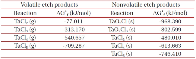
List of Gibb’s free energy of formation, ΔG˚f for the formation of etch by-products.
[Table 2.] Melting and boiling points of etch by-products at 1 atm.
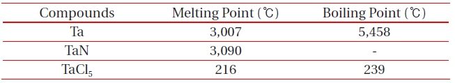
Melting and boiling points of etch by-products at 1 atm.
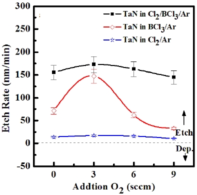
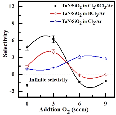
ICP etching system, the TaN thin films were etched by varying the BCl3/Ar, Cl2/Ar, and BCl3/Cl2/Ar gas chemistry. Figure 2 presents (a) the etch rates of TaN thin film and (b) the selectivity of TaN to SiO2 as a function of O2 content in the Cl2/Ar, BCl3/Ar, and BCl3/Cl2/Ar gas mixture. The other conditions of the RF power, DC-bias voltage, and process pressure were kept at 500 W, - 100 V, and 1 Pa, respectively. The maximum etch rate of the TaN thin film and the selectivity of TaN to SiO2 were 172.7 nm/min and 6.27 in the O2/BCl3/Cl2/Ar (=3:2:18:10) gas mixture, respectively. As the O2 concentration increased from 0 to 3 sccm, the etch rate of the TaN thin films and the selectivity of TaN to SiO2 increased from 155.35 to 172.7 nm/min and from 4.7 to 6.27, respectively. But, when the O2 concentration increased over 3 sccm, the etch rate of the TaN thin films and the selectivity of TaN to SiO2 decreased from 172.7 to 144.7 nm/min and from 6.27 to -1.2, respectively. Table 1 shows the Gibb’s free energy of etch products, and Table 2 shows the melting and, boiling point. In our opinion, the domination of the chemical reactions can be explained by the following factors. A) The melting point of TaCl5 is approximately 216℃, the domination of the chemical pathway may be related to its lack of volatility, by contrast, the melting point of the Ta-Cl5 is lower than the melting point of the Ta-N (=3,090℃). B) The Ta-Cl chemical bond (kJ/mol) has a lower Gibb’s free energy. The decrease of chemical bonds was due to the decreasing density of Cl radicals because the Cl atoms formed in the plasma react with TaN spontaneously [15-17].
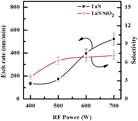
Figure 3 illustrates the etch rates of TaN thin film and the selectivity of TaN to SiO2 as a function of the RF power in the O2/BCl3/
Cl2/Ar (3:2:18:10 sccm) plasma. The other conditions of the DCbias voltage, and process pressure were - 100 V and 1 Pa, respectively. As the RF power increased from 400 to 600 W, the etch rate of TaN thin film increased from 134.15 nm/min to 521.91 nm/ min, and the selectivity of TaN to SiO2 increased from 3.63 to 6.87. Below 700 W, the results show the enhancements of the oxidation of metal nitrides, as shown in Table 1. Above 700 W, the results show the re-deposition of metal-oxygen-chlorine by-products that can be more stable than metal-chlorine by-products [18]. An increase in the RF power causes monotonic increases in both the dissociation and the ionization rates, and thus in the densities and fluxes of the O and Cl atoms and positive ions. In our case, such a layer can be resulted from both the deposition of solid B, which may bond with the surface oxygen to form BxOy, and the B and Cl radicals incorporated in the polymer-like structure [19].
Figure 4 shows the etch rate of the TaN thin film as a function of the DC-bias voltage in the O2/BCl3/Cl2/Ar (3:2:18:10 sccm) plasma. As the DC-bias voltage increases from - 50 to - 200 V, the etch rates of the TaN thin films increase from 72.63 to 581.93 nm/ min. The increase in the etch rate is attributed to the increase of the mean ion energy, resulting in an increase in the sputtering yields for both TaN and the reaction products. These results can probably be explained by the higher binding energy of the Si-O (799 kJ/mol) bond than that of the Ta-N (611 kJ/mol) bond [10].
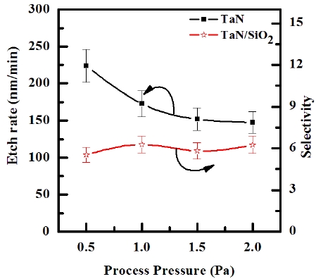
Figure 5 shows the etch rate of TaN thin film as a function of the process pressure in the O2/BCl3/Cl2/Ar (3:2:18:10 sccm) plasma. As the process pressures increased from 0.5 to 2.0 Pa, the etch rates of TaN thin film decreased from 223.7 to 147.6 nm/ min, respectively. The decrease of the process pressure enhances the density of the chemically neutral active species, which accelerates the chemical reaction [20]. Also, since the mean free path and energy of the ions increase with decreasing process pressure, the ion stimulated desorption of the reaction products is increased and the fraction of free surface available for the chemical reaction is increased. As a result of the pressure effect on the etch rate of the TaN thin film, the etch process is limited by the supply of the chemical source and, thus, the etch rate of TaN thin film increases with decreasing process pressure.
To analyze the chemical states on the surface of the etched TaN thin films exposed to the BCl3/Cl2/Ar (2:18:10 sccm) and O2/BCl3/Cl2/Ar (3:2:18:10 sccm) plasmas, the samples were investigated by XPS and AES. The input plasma parameters were set to an RF power of 500 W, DC-bias voltage of - 100 V, process pressure of 1 Pa and substrate temperature of 40℃. No boron
peaks were detected. This means that the boron and chlorine compounds are highly volatile ones such as boron-oxy-chloride (BOCl) or trichloro-boroxin (BOCl)3 [21].
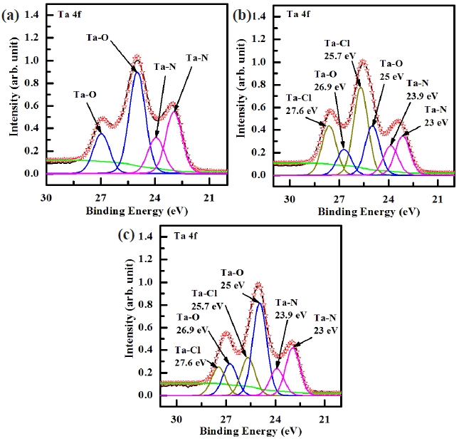
Figure 6 shows the deconvoluted peaks of the Ta 4f XPS narrow scan spectra for (a) the as-deposited films and the surface of the etched TaN thin films in (b) the BCl3/Cl2/Ar and (c) O2/ BCl3/Cl2/Ar plasma, respectively. Figure 6(a) shows the Ta 4f peak from the as-deposited TaN thin film which must originate from Ta-O and Ta-N bonds. It can be seen that the Ta 4f peak can be deconvoluted into four peaks, viz. Ta-O (25, 26.9 eV) and Ta-N (23, 24.9 eV). As shown in Fig. 6(b) and (c), it can be seen that when the TaN thin films were exposed to both the BCl3/Cl2/Ar (2:18:10 sccm) plasma and O2/BCl3/Cl2/Ar (3:2:18:10 sccm) plasma, the new peaks of Ta-Cl bonds appeared at 25.7 eV, and 27.6 eV which were higher binding energies by about ±0.7 eV. Figure 6(a) and (b) can be deconvoluted into six peaks from the etched sample. When adding O2 in BCl3/Cl2/Ar plasma, the intensity of Ta-Cl bonds decreased and the intensity of Ta-N bonds increased [22]. The XPS data provides clear confirmation that etching of the TaN thin film in the O2/BCl3/Cl2/Ar plasma results in the formation of
Ta-Ox bonds on its surface. Thus, the etch rate of TaN thin films was decreased when the O2 concentration increased over 3 sccm.
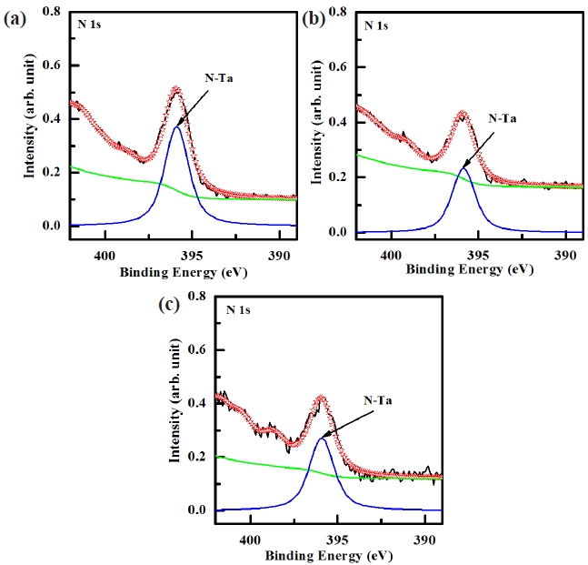
Figure 7 shows the deconvoluted peaks of the N 1s XPS narrow scan spectra for (a) the as-deposited films and the surface of the etched TaN thin films in (b) the BCl3/Cl2/Ar and (c) O2/BCl3/ Cl2/Ar plasma, respectively. For the N 1s peak, the peak at 395.9 eV corresponded to that of N-Ta, which originated from the interface of the TaN thin film. As shown in Fig. 7 (b) and (c), the shoulder peaks of N-Ta (395.9 eV) was decreased significantly in the BCl3/Cl2/Ar and O2/BCl3/Cl2/Ar plasma as a result of the preferential removal of Ta and N. However, when the TaN thin films were etched in the BCl3/Cl2/Ar and O2/BCl3/Cl2/Ar plasma, the N 1s peak intensity at 395.9 eV was decreased due to the formation of Cl-N bonds [23]. The intensity of the N 1s peck for the surface of the etched TaN thin film in O2/BCl3/Cl2/Ar plasma was higher than that of the etched TaN thin film in the BCl3/Cl2/Ar plasma. This is due to the dramatic increase in the number of Cl-N bonds, which resulted from the effective dissociation of the Ta-N bonds by the ion bombardment. Based on the XPS result, it was revealed that Ta and N were removed by the chemical reactions with the Cl radicals and the physical bombardment of the Ar ions [24-26].
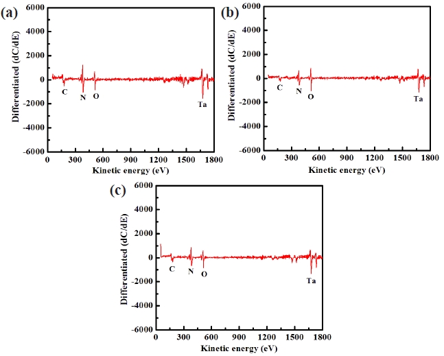
Figure 8 shows the AES surface scan spectra of the TaN thin film for (a) the as-deposited films and the surface of the etched TaN thin films in (b) the BCl3/Cl2/Ar and (c) O2/BCl3/Cl2/Ar plasma, respectively. The etching time of the TaN thin film was 10 sec. Figure 8(a) shows an AES surface scan of the as-deposited TaN thin film in which O peaks are detected. The origin of carbon elements are a result of the contamination in the etching chamber or the air. After etching, the B and Cl-related peaks were not observed. With the addition of O2 gas, the intensity of N peaks increased compared to that of the etched sample in BCl3/ Cl2/Ar plasma. This result means that by-products such as Ta-Ox increased on the etched surface in O2/BCl3/Cl2/Ar plasma. Therefore, the XPS and AES data clearly show that the surface of the etched TaN thin films in O2/BCl3/Cl2/Ar plasma is formed with nonvolatile etch products such as Ta-Ox and Ta-Clx.
The etching characteristics of the TaN thin film were investigated in O2/BCl3/Cl2/Ar plasma. The maximum etch rate of the TaN thin film was 172.7 nm/min in the O2/BCl3/Cl2/Ar (=3:2:18:10) gas mixture. As the O2 fraction in the O2/BCl3/Cl2/ Ar plasma was increased from 0 to 3 sccm, the etch rate of TaN thin film increased. In addition, the passivation layer formation on the sidewall also increased due to a small amount of O2. However, the etch rate of the TaN thin film decreased with the further addition of O2 gas. The chemical states of the etched TaN thin films were investigated using XPS. The etching mechanism of the TaN thin film can be explained as follows: Ta interacted with the Cl radicals in the Cl2 containing plasmas, but remained at the surface due to the low volatility of Ta-Clx, which could be effectively removed with the help of ion bombardment.