검색 전체 메뉴
PDF
맨 위로
OA 학술지
Performance-determining factors in flexible transparent conducting single-wall carbon nanotube film
  • 비영리 CC BY-NC
  • 비영리 CC BY-NC
ABSTRACT
Performance-determining factors in flexible transparent conducting single-wall carbon nanotube film
KEYWORD
single-wall carbon nanotube , transparent conducting film , dip coating method
  • 1. Introduction

    Flexible transparent conducting films (TCF) are technologically important for future wearable displays. Although present indium-tin-oxide thin films have excellent electrical properties and high optical transmittance, their flexibility upon bending is extremely poor. Therefore, development of an alternative material with high mechanical flexibility is highly desired. Carbon nanotubes (CNTs) have been recently proposed as a promising candidate to satisfy the desired flexibility, owing to their high aspect ratio and excellent elastic property, in addition to high electrical conductivity [1-3]. Consequently, the fabrication of flexible TCFs with CNTs has recently been carried out. These recent studies have shown that the electrical conductivity and optical transmittance of CNT films varies, depending on the coating methods and the intrinsic properties of the CNTs [4-14]. In general, the performance of CNT-based TCFs are typically governed by the inherent properties of the CNTs, such as purity, defect concentration, and electrical conductivity. Efforts have been made to associate material-induced factors with better TCF performance [1,15]. However, the characteristics of CNT-based TCFs are still not clear due to a lack of systematic studies on the relationship between preparation conditions and film properties. The performance of CNT-based TCFs depends strongly on the higher order structure of the CNTs, such as entangled and bundle structures. This feature could be evaluated while investigating the performance-determining factors for designing better TCFs.

    We assume that the performance of CNT-based TCFs directly depends on the number of intersecting, interconnected CNT bundles, and the coverage of SWCNTs on the substrate. In this study, we microscopically and macroscopically evaluated the performance of TCFs to elucidate performance-determining factors, by using experimental results of single-wall CNTs (SWCNTs)-coated TCFs on flexible polyethylene terephthalate (PET) film prepared by dip-coating process [14].

    2. Experimental Details

    Highly pure SWCNTs synthesized by arc discharge process were purchased from Iljin Nanotech. The SWCNT diameters were in the range of 1.4 to 1.5 nm with a length of 5 to 20 μm. Thermogravimetric analysis profile gave 1.3 wt% of metal catalyst.

    The purified SWCNTs were well dispersed in 1,2-dichloroethane (DCE) solvent without additives [14,16,17]. The low vaporization temperature of DCE (83.5℃) allows more SWCNT to be deposited on the substrate. Ten milligram of SWCNTs were immersed in 100 mL of DCE solvent. These were then sonicated in a bath type sonicator for 500 min at room temperature, followed by centrifugation at a speed of 6800 rpm for 10 min. The supernatant was decanted and sonicated prior to film formation. The PET substrate was sonicated in acetone for 10 min and then washed with deionized water to clean the substrate surface. The PET substrate was vertically positioned above a container of the SWCNT-dispersed DCE solution and then immersed into the SWCNT solution for 2 s, and withdrawn upward, with a continuous speed of 50 mm/min. Then, the PET substrate was dried for 5 s. This procedure was repeated between 100 to 400 times. The dip-coating was conducted in a glove box in Ar atmosphere in order to avoid moisture adsorption into the DCE solvent.

    Field emission scanning electron microscopic (FE-SEM) images of the SWCNT-based TCFs were obtained with a JSM-63301 (JEOL). Their electrical conductance was measured using a four-point probe method. Optical transmittance was measured using UV-visible spectrometry (Carry 5000) in the range of 400 to 800 nm.

    3. Results and Discussion

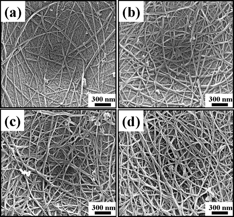
    Fig. 1 presents the FE-SEM images of SWCNT network films on the PET substrate as a function of the different number of dippings. With increasing number of dippings, the amount of coated SWCNTs increases considerably. However, the coating of the PET substrate is not enough after a dipping treatment of 100 times, although the DCE completely wets the PET substrate.

    The DCE solvent is easily evaporated from the substrate, depositing the SWCNTs film on it. The SWCNT film consists of a network having many intersection points. The intersection points in the TCF film are a crucial factor for good electrical conductivity of the film. The FE-SEM images of SWCNTcoated TCFs according to dipping treatment number show that the number of intersection points increases significantly with the number of dippings. The percolation threshold should reach a minimum amount of SWCNT deposits to maximize optical transmittance [18-20].

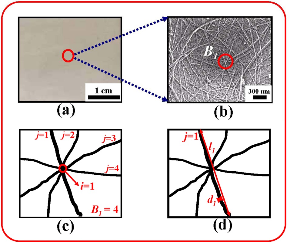
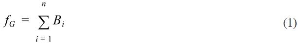
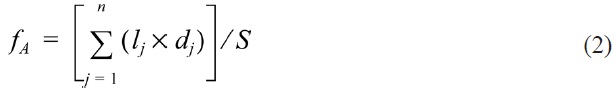
    Fig. 2 shows a schematic representation for estimating the performance-determining factors of the TCFs using the observed FE-SEM images. Figs. 2a and b show an optical image and an

    FE-SEM image after 100 dippings. We defined two factors that govern the SWCNT-TCF performance. First, the electrical conductance of the film is closely related to the intersection points in the SWCNT network; the electrical conductance of the SWCNT network film should be simply proportional to the number of intersection points of SWCNT bundles, and the number of SWCNT bundles that are interconnected at each intersection point. Therefore, we first define the conductance factor fG as follows.

    image

    where Bi is the number of interconnected SWCNT bundles (j) at each intersection point (i), as illustrated in Fig. 2c. Therefore, fG is the sum of Bi at the intersection point (i). Second, the absorbance of the film is proportional to the coverage of SWCNTs on the substrate. Therefore, we also define the absorbance factor fA, which is given by Eq. (2).

    image

    where lj and dj are the length and diameter of the j-th SWCNT bundle in the FE-SEM image, respectively, as illustrated in Fig. 2d, and S is the total area of the FE-SEM image.

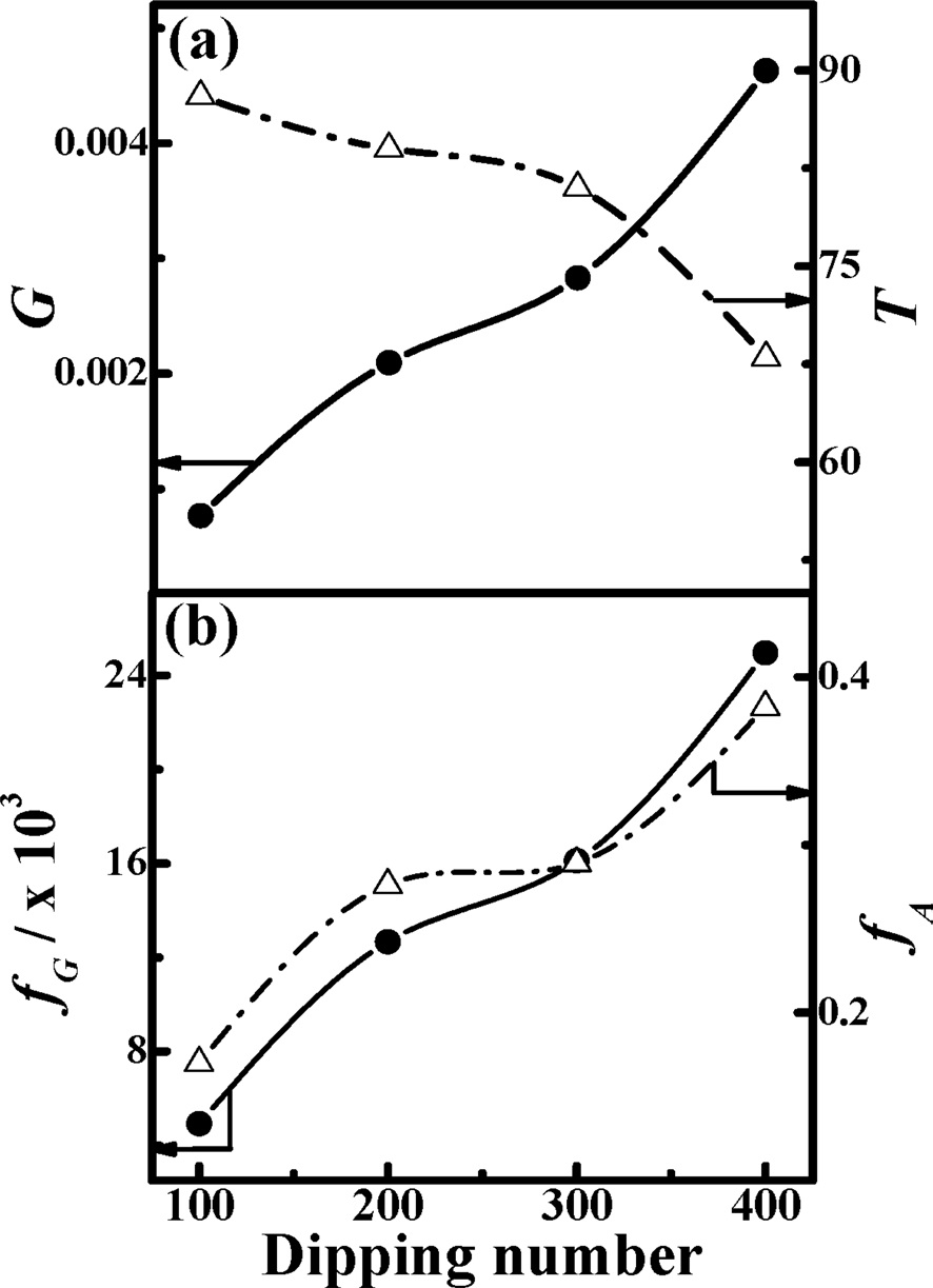
    Fig. 3a shows the changes of electrical conductance (G) and optical transmittance (T) of dip-coated SWCNT-TCFs with the number of dippings. With the increasing number of dippings, the electrical conductance of the SWCNT-TCFs increases, accompanied by a reduction of the optical transmittance; this is ascribed to the increase in the number of SWCNT intersection points and the coverage of SWCNTs on the substrate. The conductance (fG) and absorbance (fA factors determined by Eqs. (1) and (2) are shown in Fig. 3b. Since the optical transmittance is inversely proportional to the absorbance, the change of fAvalue with the number of dippings has an opposite tendency to that of the T value. Both higher conductance and transmittance are simultaneously desired for better film performance. We need a film property factor including both properties. Thus, we define the microscopic film property factor (QMic), as given by Eq. (3).

    image

    QMic can be compared with the macroscopic film property factor (QMac) expressed with the measured electrical conductance (G) and optical transmittance (T), as given by Eq. (4).

    image

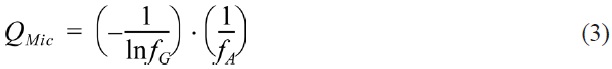
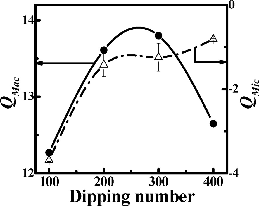
    Fig. 4 presents the comparison of QMic with QMac as a function of the number of dippings. QMac shows a sharp increase up to 200 dipping times and then decreases at 300 dipping times. Although the electrical conductance was increased, the optical transmittance decreased rapidly at a large number of dippings. As a consequence, the film performance is degraded. The QMic resembled the QMac in a similar way up to 300 dipping times. It should be noted, at a large number of dippings, counting the number of intersection points in the SWCNT network becomes ambiguous because these numbers increase very rapidly, as shown in Fig. 1. Thus the errors in counting these numbers dominate, making the data point uncertain.

    4. Conclusions

    In summary, SWCNT-TCFs were fabricated by dip-coating method. Our dip-coating approach provided reasonable quality SWCNT-TCF films. The film’s microscopic property factor was defined by the number of interconnected SWCNT bundles at intersection points, and the coverage of SWCNTs on the substrate, in FE-SEM images. The microscopically extracted film property factors are in good agreement with macroscopically obtained values, especially for a small number of dippings. Our results clearly revealed that a sparsely entangled random network structure with a sufficient number of intersection points and a minimum SWCNT coverage is a key factor for improving SWCNT-TCF performance. However, the dispersion of SWCNTs is also an important factor influencing SWCNT-TCF performance. Therefore, dispersing SWCNT bundles into individual SWCNTs, or into a smaller bundle size, is desired to improve TCF electrical conductance and optical transmittance.

참고문헌
  • 1. Wu Z, Chen Z, Du X, Logan JM, Sippel J, Nikolou M, Kamaras K, Reynolds JR, Tanner DB, Hebard AF, Rinzler AG. (2004) Transparent, conductive carbon nanotube films. [Science] Vol.305 P.1273 google cross ref
  • 2. Cao Q, Hur SH, Zhu ZT, Sun YG, Wang CJ, Meitl MA, Shim M, Rogers JA. (2006) Highly bendable, transparent thin-film transistors that use carbon-nanotube-based conductors and semiconductors with elastomeric dielectrics. [Adv Mater] Vol.18 P.304 google cross ref
  • 3. Fanchini G, Unalan HE, Chhowalla M. (2006) Optoelectronic properties of transparent and conducting single-wall carbon nanotube thin films. [Appl Phys Lett] Vol.88 P.191919 google cross ref
  • 4. De Volder MFL, Tawfick SH, Baughman RH, Hart AJ. (2013) Carbon nanotubes: present and future commercial applications. [Science] Vol.339 P.535 google cross ref
  • 5. Park HG, Lee MJ, Kim K, Seo DS. (2012) Transparent conductive single wall carbon nanotube network films for liquid crystal displays. [ECS Solid State Lett] Vol.1 P.R31 google cross ref
  • 6. Yang Y, Jeong S, Hu L, Wu H, Lee SW, Cui Y. (2011) Transparent lithiumion batteries. [Proc Natl Acad Sci U S A] Vol.108 P.13013 google cross ref
  • 7. Zhang M, Fang S, Zakhidov AA, Lee SB, Aliev AE, Williams CD, Atkinson KR, Baughman RH. (2005) Strong, transparent, multifunctional, carbon nanotube sheets. [Science] Vol.309 P.1215 google cross ref
  • 8. Lee SH, Teng CC, Ma CCM, Wang I. (2011) Highly transparent and conductive thin films fabricated with nano-silver/double-walled carbon nanotube composites. [J Colloid Interface Sci] Vol.364 P.1 google cross ref
  • 9. Kim MJ, Shin DW, Kim JY, Park SH, Han It, Yoo JB. (2009) The production of a flexible electroluminescent device on polyethylene terephthalate films using transparent conducting carbon nanotube electrode. [Carbon] Vol.47 P.3461 google cross ref
  • 10. Shin EC, Jeong GH. (2011) Fabrication of transparent, flexible and conductive films using as-grown few-walled carbon nanotubes. [Curr Appl Phys] Vol.11 P.S73 google cross ref
  • 11. Meitl MA, Zhou Y, Gaur A, Jeon S, Usrey ML, Strano MS, Rogers JA. (2004) Solution casting and transfer printing single-walled carbon nanotube films. [Nano Lett] Vol.4 P.1643 google cross ref
  • 12. Saran N, Parikh K, Suh DS, Munoz E, Kolla H, Manohar SK. (2004) Fabrication and characterization of thin films of single-walled carbon nanotube bundles on flexible plastic substrates. [J Am Chem Soc] Vol.126 P.4462 google cross ref
  • 13. Shimoda H, Oh SJ, Geng HZ, Walker RJ, Zhang XB, McNeil LE, Zhou O. (2002) Self-assembly of carbon nanotubes. [Adv Mater] Vol.14 P.899 google cross ref
  • 14. Song YI, Yang CM, Kim DY, Kanoh H, Kaneko K. (2008) Flexible transparent conducting single-wall carbon nanotube film with network bridging method. [J Colloid Interface Sci] Vol.318 P.365 google cross ref
  • 15. Pasquier AD, Unalan HE, Kanwal A, Miller S, Chhowalla M. (2005) Conducting and transparent single-wall carbon nanotube electrodes for polymer-fullerene solar cells. [Appl Phys Lett] Vol.87 P.203511 google cross ref
  • 16. Kim KK, Bae DJ, Yang CM, An KH, Lee JY, Lee YH. (2005) Nanodispersion of single-walled carbon nanotubes using dichloroethane. [J Nanosci Nanotechnol] Vol.5 P.1055 google cross ref
  • 17. Song YI, Kim GY, Choi HK, Jeong HJ, Kim KK, Yang CM, Lim SC, An KH, Jung KT, Lee YH. (2006) Fabrication of carbon nanotube field emitters using a dip-coating method. [Chem Vap Depos] Vol.12 P.375 google cross ref
  • 18. Hu L, Hecht DS, Gruner G. (2004) Percolation in transparent and conducting carbon nanotube networks. [Nano Lett] Vol.4 P.2513 google cross ref
  • 19. Unalan HE, Fanchini G, Kanwal A, Du Pasquier A, Chhowalla M. (2006) Design criteria for transparent single-wall carbon nanotube thin-film transistors. [Nano Lett] Vol.6 P.677 google cross ref
  • 20. Darhuber AA, Troian SM, Davis JM, Miller SM, Wagner S. (2000) Selective dip-coating of chemically micropatterned surfaces. [J Appl Phys] Vol.88 P.5119 google cross ref
OAK XML 통계
이미지 / 테이블
  • [ Fig. 1. ]  Field emission scanning electron microscopic images of singlewalled carbon nanotube network film coated with different dipping number; (a) 100, (b) 200, (c) 300, and (d) 400 times.
    Field emission scanning electron microscopic images of singlewalled
carbon nanotube network film coated with different dipping
number; (a) 100, (b) 200, (c) 300, and (d) 400 times.
  • [ Fig. 2. ]  (a) Optical image, (b) field emission scanning electron microscopic image after 100 dipping times, and schematic representations for determining (c) conductance factor (fG) and (d) absorbance factor (fA) in B1 of (b).
    (a) Optical image, (b) field emission scanning electron microscopic
image after 100 dipping times, and schematic representations for
determining (c) conductance factor (fG) and (d) absorbance factor (fA) in B1
of (b).
  • [ Fig. 3. ]  (a) Electrical conductance (G) and optical transmittance (T) and (b) the conductance (fG) and absorbance (fA) factors of single-walled carbon nanotube-transparent conducting films as a function of the number of dipping.
    (a) Electrical conductance (G) and optical transmittance (T) and
(b) the conductance (fG) and absorbance (fA) factors of single-walled carbon
nanotube-transparent conducting films as a function of the number
of dipping.
  • [ Fig. 4. ]  Comparison of the microscopic film property factor (QMic) with macroscopic film property factor (QMac) as a function of the number of dipping.
    Comparison of the microscopic film property factor (QMic) with
macroscopic film property factor (QMac) as a function of the number of
dipping.
(우)06579 서울시 서초구 반포대로 201(반포동)
Tel. 02-537-6389 | Fax. 02-590-0571 | 문의 : oak2014@korea.kr
Copyright(c) National Library of Korea. All rights reserved.