The effect of diffusing substrate and pillow lenses on the outcoupling efficiency of organic light-emitting diodes (OLEDs) was studied by optical simulation based on the point-dipole model. The diffusing substrate included Mie scatterers by which the condition of total internal reflection could be broken. The finite-difference time-domain method was used to obtain the intensity distribution on the transparent electrode of an OLED, which was used as a light source to carry out a ray-tracing simulation of the OLED and the diffusing substrate. It was found that the outcoupling efficiency of the OLED was sensitive to the thickness of organic layers and could be increased by 21.0% by adopting a diffusing substrate in which Mie scatterers whose radius was 2.0 μm were included at the density of 107 mm-3 and by 65.5% by forming one pillow lens with the radius of 2 mm on the front surface of the glass substrate. This study revealed that the outcoupling efficiency could be improved by adopting diffusing substrate and pillow lenses along with the optimization of the thickness of each layer in the OLED.
OLEDs have recently attracted great attention due to their excellent performance in display devices and illumination devices [1,2]. Visible light is generated from the organic emitting layer, where the injected holes and electrons recombine. However, a substantial portion of the generated light is trapped in the organic layers and the glass substrate because of their high refractive indices [3]. Many attempts have been made to improve the outcoupling efficiency (OCE) of OLEDs [1-5], one of which is to apply a diffusing structure [6-9]. Using a glass substrate as a diffusing layer in OLEDs may be very cost-effective in many outcoupling designs. In our previous study [10], we reported the optical simulation results for an OLED with a scatterer-included glass substrate based on a ray-tracing technique. It was shown that the incorporation of Mie scatterers into the glass substrate increased the OCE substantially. However, the ray-tracing technique has some limitations in simulating the optical performance of OLEDs because the thicknesses of the organic layers and the transparent indium-tin-oxide (ITO) layer are on the order of 100 nm, which is much smaller than the wavelength of visible light. In this respect, more rigorous analysis is necessary to simulate OLEDs, such as through the finitedifference time-domain (FDTD) method [11,12]. The purpose of this study was to investigate the effect of a diffusing substrate (a glass substrate into which Mie scatterers are incorporated) on an OLED structure by combining FDTD and ray-tracing methods.
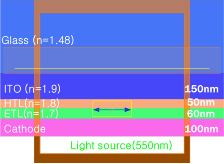
Figure 1 shows a schematic structure of the OLED studied by the FDTD method to calculate the electromagnetic waves propagating through the planar structure. A commercially available software (FDTD Solutions, Lumerical Solutions, Vancouver, Canada) was used to carry out the simulation. The OLED in Fig. 1 is a bottom-emitting type consisting of a metal cathode, an electron-transporting layer (ETL), a hole-transporting layer (HTL), an ITO layer and a glass substrate. The simulation area was 10×10 μm2. The refractive indices of these layers were the same as those reported in Ref. [3]. A point-dipole radiation source at a wavelength of 550 nm was placed at the center of the interface between the HTL and ETL. The oscillation direction of the point dipole was set along the three orthogonal directions, two in the OLED plane and one normal to the OLED plane. The far-field angular radiant intensity distribution on the ITO layer was imported into the ray-tracing software program (ASAP, Breault Research Organization, Tucson, USA) as the emitting ray distribution of an imaginary flat light source. This imaginary light source, with an area of 0.5×0.5 mm2, was located at the center of the glass substrate. A glass substrate with an area of 2×2 mm2 and a thickness of 0.7 mm acted as the diffusing layer into which scattering particles were incorporated.
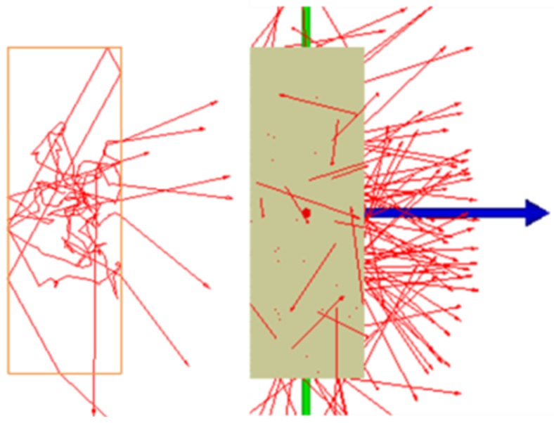
Figure 2 shows a schematic structure of the OLED glass substrate studied by the ray-tracing method. As shown, the
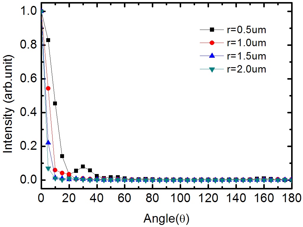
rays are randomly scattered and change directions abruptly in the glass substrate. The particles incorporated into the glass substrate behaved as Mie scatterers. Fig. 3 shows the scattering intensity of the incident light as a function of the scattering angle at a few particle radii. If the particle radius approaches the wavelength of the visible light, the distribution of the forward scattering becomes broad and small oscillatory peaks are observed at high angles, which can be obtained from classical electromagnetic theory.
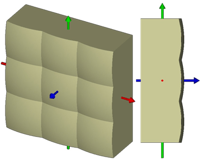
Pillow-shaped lenses were placed on the front surface of the glass substrate to further increase the OCE. The surface was modified to increase the critical angle and thus, decrease the loss of light by total internal reflection. The radius was optimized, and the configuration of pillow lenses on the glass substrate was varied among 1×1, 3×3 and 5×5 arrays. Fig. 4 shows the case of a 3×3 array of pillow lenses.
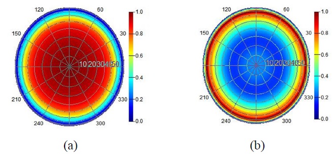
Figure 5 (a) and (b) show a polar plot of the far-field intensity distribution proportional to |
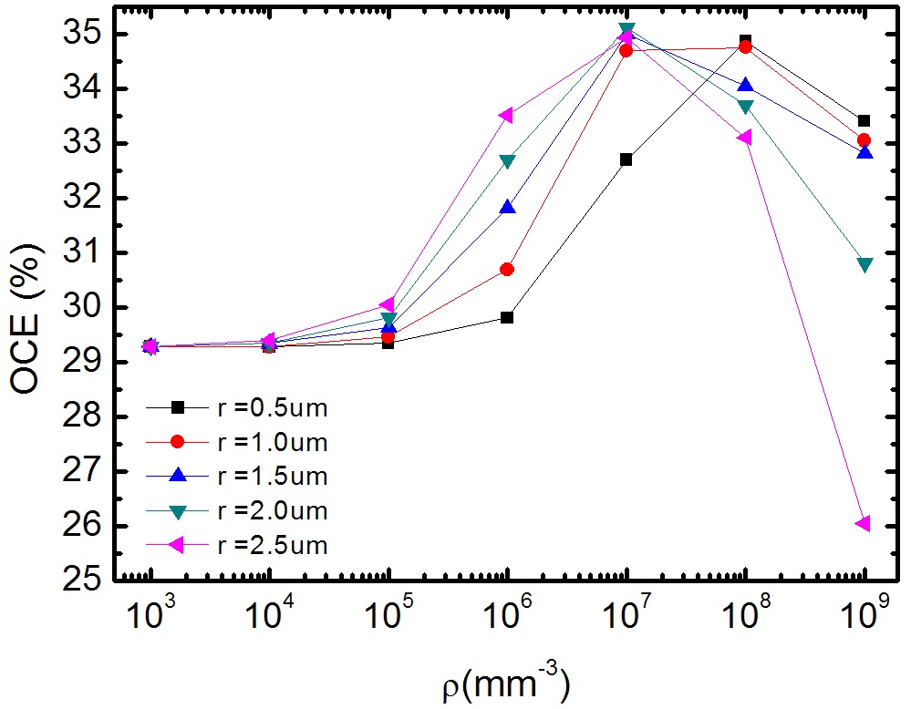
Figure 6 shows the dependence of the OCE on the density and the radius of the Mie scatterers embedded in the glass substrate. This result clearly shows that the OCE displays a maximum at a certain particle density of 107~108 mm-3 depending on the particle radius. If the density is too low, the scattering effect is not sufficient to disturb the rays propagating through the glass substrate, resulting in almost no increase in the outcoupling efficiency. Conversely, if the density is too high, light cannot propagate easily due to excessively large scattering events, resulting in a decrease in the efficiency. Similar results were reported in Ref. [13]
for a scattering layer inserted between a normal glass substrate and an ITO coating. The maximum OCE achieved was approximately 34.9~35.1% at a density of 107 mm-3 and a radius of 1.5~2.5 μm.
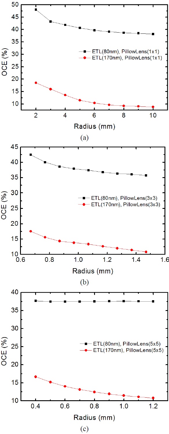
Figure 7 shows the OCE as a function of the radius for
the three cases, i.e., (a) 1×1, (b) 3×3 and (c) 5×5 pillow lens arrays. It is worth noting that the OCE is very sensitive to the ETL thickness. The placement of pillow lenses on the front surface of the glass substrate increases the OCE from 35% to a maximum of ~48% at
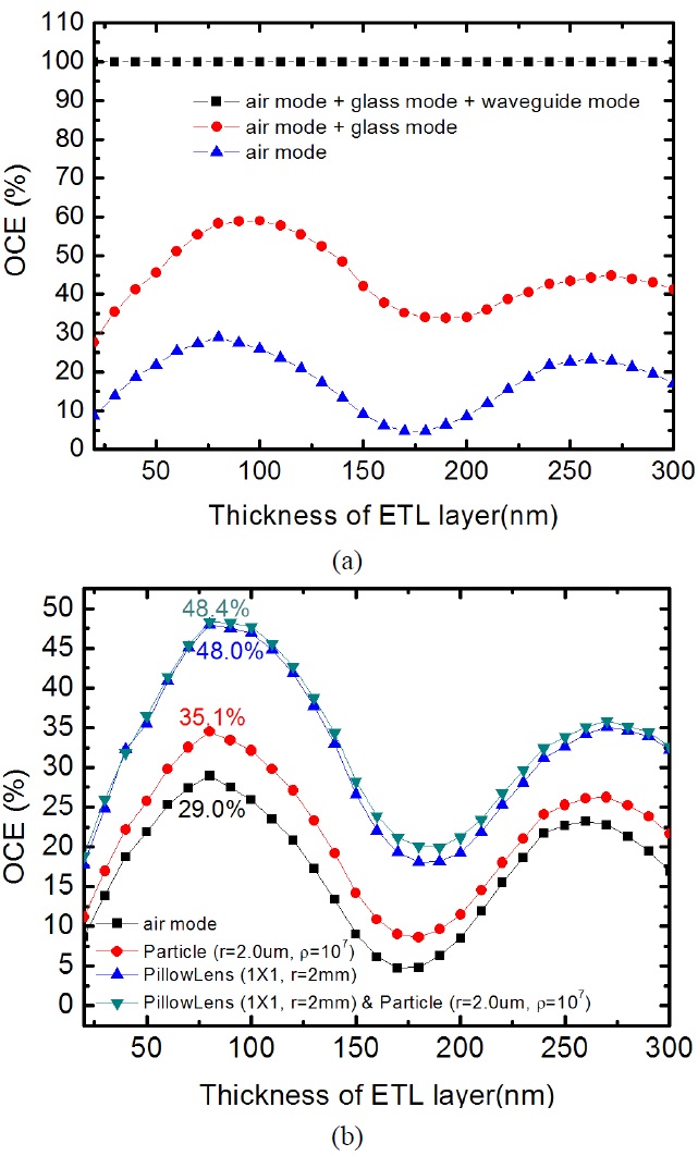
Figure 8 shows the dependence of the ratio in each of the three modes (waveguide mode, glass mode, and the air mode) on the thickness of ETL. The waveguide and glass modes are indicative of the light trapped in the organic layer and the glass substrate, respectively. Here, the waveguide mode partly includes cathode loss, sometimes called surface plasmon loss. The air mode represents the amount of light that escapes from the OLED and thus determines the outcoupling efficiency. The ratios of these three modes depend significantly on the ETL thickness and show some oscillation. The air mode exhibits two maxima at approximately 80 and 260 nm within the examined thickness range. This result is very similar to the results of previous calculations and simulations [12,14]. As shown in Fig. 8, the OCE becomes much weaker at
The maximum value of the OCE can be increased by incorporating scattering particles into the glass substrate. Fig. 8 (b) shows that the maximum OCE at approximately 80 nm increases from 29.0% to 35.1% when the density of the scattering particle at the radius of 2.0 μm is 107 mm-3. If one pillow lens with the radius of 2 mm is added to the substrate without scattering particles, the maximum OCE increases to 48.0%. However, the combination of pillow lenses and scattering particles results in a minute increase in the OCE of 0.4%, indicating that the pillow lens structure is much more effective in outcoupling the light guided in OLED into the air. Finally, we should note that the change in the thicknesses of the HTL and ITO also results in similar oscillatory behavior for the OCE because these layers control the allowed number of modes in the waveguide, which consisted of an ETL, an HTL and ITO [12]. However, the most drastic change is usually observed after modifying the ETL thickness because the distance between the location of the radiating dipole and the cathode, which is determined
by the ETL thickness is the most important parameter affecting the microcavity effect of OLEDs [16].
The increase in the OCE by adopting scattering particles in the substrate was experimentally demonstrated by previous studies [13,17-18]. Barthelt et al., reported that the application of scattering films on the glass substrate could increase the OCE by approximately 22% [18], which is close to the value obtained by this study. In some studies [13,17], the refractive index of the substrate was controlled to be close to that of ITO/organic layers. In this case, the trapped waveguide mode can also be extracted via scattering resulting in much higher OCE, because there is nearly no index barrier between the substrate and the ITO/organic layers. On the other hand, there have been many studies on the effect of lenses on the OCE [19-21]. Application of a hemi-spherical lens on the substrate was found to increase the OCE by 1.6~3.0 depending on the refractive index and lens parameters [19]. Using a single lens on OLEDs, however, increases the thickness of the OLED device. In this context, microlens-based optical structures are preferred for practical applications [20-21]. Compared to the microlenses of which the cross-section is circular on the substrate, the fill factor of pillow lenses, which is 100%, is much higher. Therefore, it would be interesting to compare systematically the optical performances of various microlenses with different fill factors. In addition, the intensity distribution on OLED is expected to depend on the detailed shape of microlenses and other optical structures adopted for enhancing OCE. The far-field intensity distribution depending on the scattering particles and pillow lenses was investigated and will be reported elsewhere [22].
Finally, we would like to point out that an isotropic point dipole was assumed for the simulation. However, it is now widely recognized that the emitter orientation is closely related to the coupling between the surface plasmons and the radiating dipole and thus has substantial effect on the device efficiency [2]. In this respect, polarization-dependent optical modeling and analysis [23] are important for getting more insights into the optical power distribution in OLEDs, which is under progress and will be reported in the forthcoming article.
The effect of the density and the radius of Mie scatterers embedded in a glass substrate on the outcoupling efficiency of an OLED was studied using optical simulation. The finite-difference time-domain method was used to obtain the intensity distribution on the transparent electrode of the OLED. This distribution was in turn used as a light source to carry out a ray-tracing simulation of the OLED with a diffusing substrate. The OCE was found to be very sensitive to the thickness of the ETL, which was related to the change in the number of allowed waveguide modes in the organic layer. The incorporation of Mie scatters with a radius of 2.0 μm into the glass substrate at the density of 107 mm-3 increased the OCE by 21.0%. Application of one pillow lens with a radius of 2 mm on the front surface of the glass substrate increased the OCE by 65.5%. The present simulation study revealed that the OCE of bottom-emitting OLEDs could be enhanced by adopting scattering substrate or pillow lenses formed on the substrate, which should be combined by the optimization of the thicknesses of each layer in OLED, in particular, the electron-transporting layer.