Various wireless communication standards, such as wireless local area networks (WLANs), worldwide interoperability for microwave access (WiMAX), wideband code division multiple access (W-CDMA), long-term evolution (LTE), etc., have been developed throughout the world and more standards will likely emerge in the near future. The integration of separate standards into one unit increases the size, cost, and complexity of wireless systems. The need for the design of low-cost, compact robust radio frequency components such as tunable bandpass filters (BPFs) operating at multiple frequency bands to meet the demands of next generation wireless systems have become apparent.
In some applications of wireless communication systems, radios themselves sense the available spectrum and decide on the communications channel (frequency, bandwidth, and modulation scheme) to be used. Therefore, it is important to design a multi-band BPF with a tunable center frequency and bandwidths. To meet these requirements, various approaches have been applied to design tunable BPFs using different kinds of tuning devices, such as micro-electromechanical system (MEMS) devices [1,2], ferroelectric devices/capacitors [3], PIN diodes [4], and semiconductor varactor diodes [5-9]. These tuning devices allow tunability of the center frequency of filters by changing the effective length of their resonators and the variation of the bandwidth by changing coupling between resonators.
Semiconductor varactors are widely used in designing tunable BPFs due to high tuning speed and reliability [5-9]. In comparison to the design of single-band tunable filters, only a limited number of studies have been undertaken to design filters with a tunable center frequency and bandwidth independent of one another [10,11]. There have been some attempts to design tunable dual-passband filters [12,13]. However, no studies have addressed the design of a tunable dual-band BPF with independently tunable center frequencies and bandwidths.
With the tunable passband frequency, the harmonic bands that degrade the out-of-passband characteristics are also tuned. Thus, the suppression of harmonics is one of the critical issues related to tunable filters. This issue has rarely been addressed in the design of tunable dual-band filters.
In this paper, dual-band BPFs with independently tunable passband center frequencies and bandwidths are presented. From theoretical even- and odd-mode analysis, it is found that the passband center frequencies can be varied by controlling the odd- and even-mode resonant frequencies. The separation between the odd- and even-mode resonant frequencies is proportional to the bandwidths of passbands; these can be controlled independently by the even-mode resonant frequencies by keeping the odd-mode resonant frequencies constant. To suppress the harmonics, the defected ground structure (DGS) is used at the input/output feeding lines. The band-rejection characteristics of the DGS are utilized to suppress the harmonics of the proposed BPF.
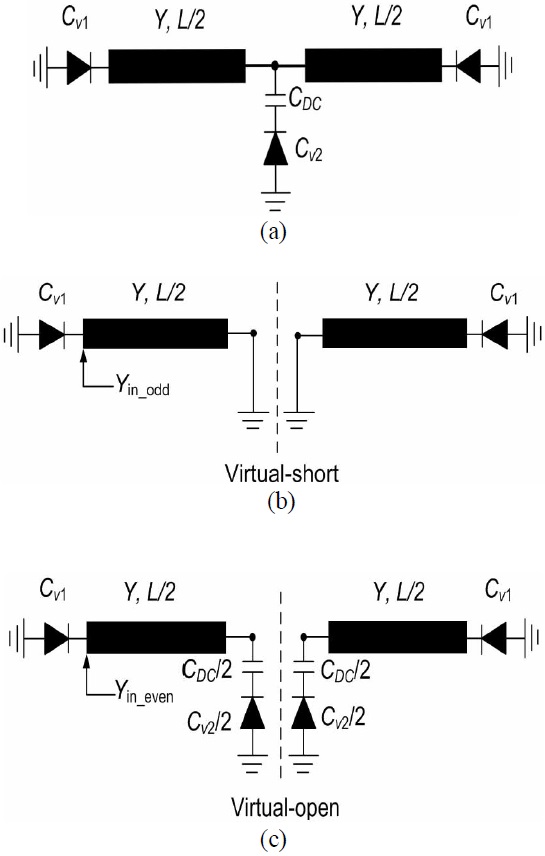
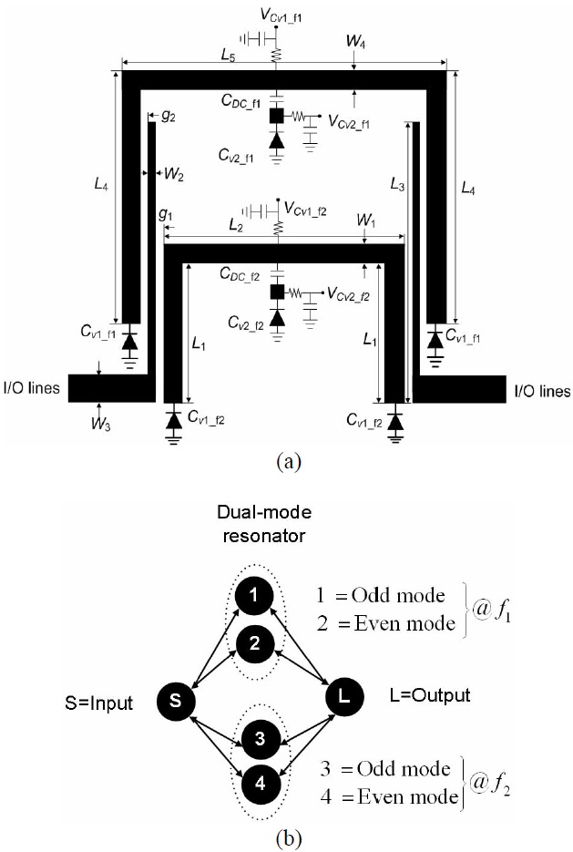
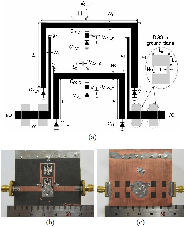
Fig. 1(a) shows the proposed two-pole varactor-tuned dual-band BPF. It consists of two single-band BPFs combined with common input and output ports. Each single- band BPF comprises dual-mode resonators that contain a transmission line and three varactor diodes. The coupling scheme of the proposed filter is shown in Fig. 1(b), where
Fig. 2(a) shows the basic structure of the proposed resonator. Two varactor diodes are the attached at ends of the transmission line with tunable capacitances
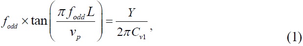
where
For even-mode excitation, there is no current flowing through the center of the transmission line. Under this condition, the proposed resonator can be represented by the equivalent half circuit shown in Fig. 2(c). For the resonance condition, the even-mode resonant frequency can be determined as follows:
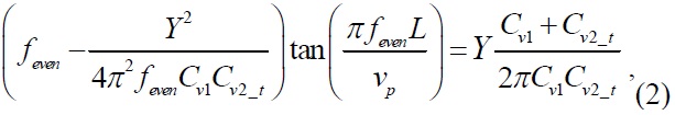
where
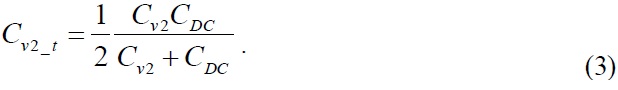
From (2) and (3), it can be observed that the evenmode resonant frequency depends on
To verify the theoretical analysis, a full-wave electromagnetic (EM) simulation was carried out using HFSS
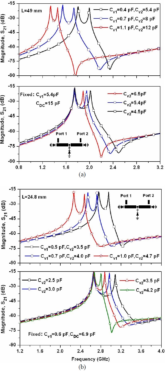
Fig. 3 shows the simulated resonant characteristics according to different capacitances (
First, the requirement of the ideal dual-mode filter at each passband should be determined; this may be derived from its fixed frequency response centering at the high-frequency edge of a given tuning range. Then the separation of odd- and even-mode resonant frequencies and the required
Second, the tuning rate of the odd-and even-mode resonant frequencies should be determined by selecting
To demonstrate the described design method, filter centerings at
2. Analysis of Center Frequency and Bandwidth Tunability
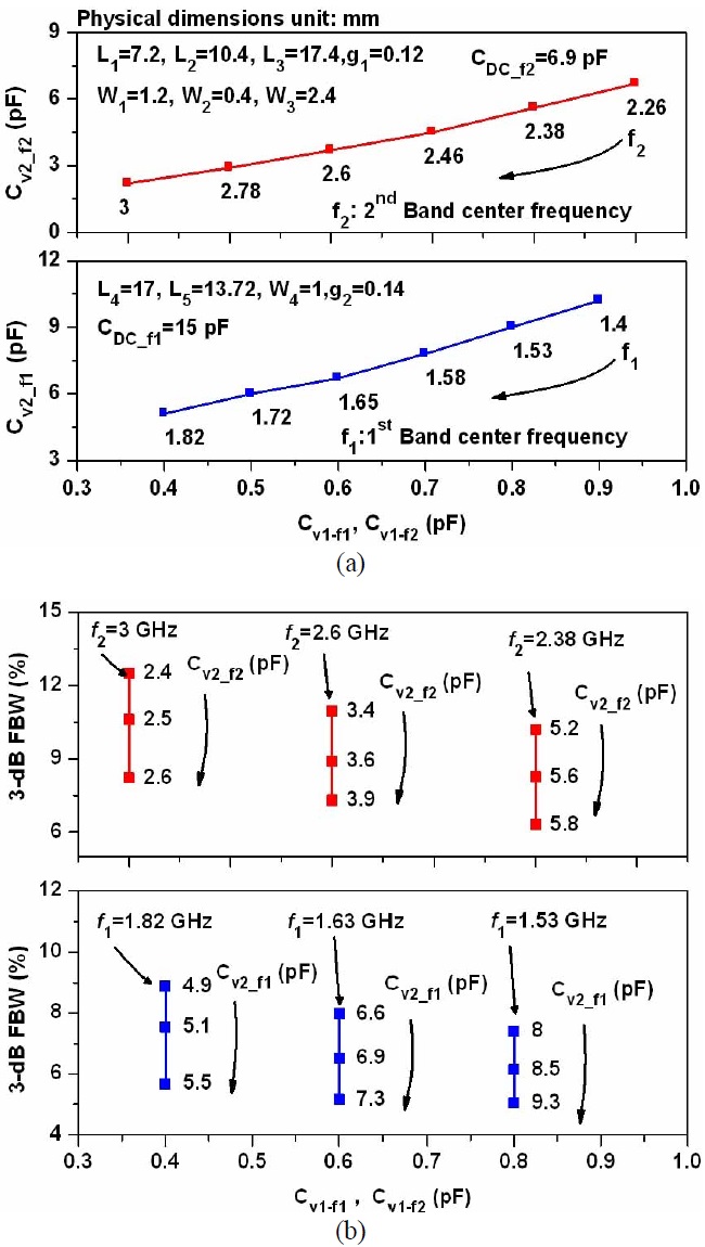
Fig. 4(a) presents the tunability of center frequency of passbands according to capacitances
Fig. 4(b) presents the 3-dB FBWs verses capacitances (keeping
Ⅲ. Simulation and Measurement Results
To verify the analysis of the proposed resonators, two types of tunable dual-band BPF were designed, simulated, and measured. Fig. 1(a) depicts the configuration of microstrip dual-mode tunable dual-band filter I. In the proposed filter, two dual-mode resonators are combined with common input/output ports. The inner resonators are designed for higher passbands, whereas the outer resonator is designed for lower passbands. The resonators are folded in order to reduce the size. The substrate is RT/Duriod 5880 made by Rogers with a dielectric constant (
The proposed filter employs two types of varactor diodes from Skyworks: SMV1231-011LF for tuning
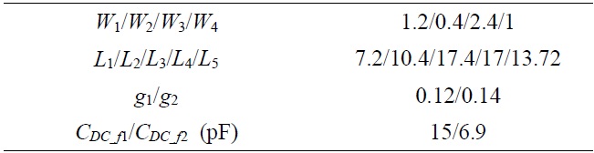
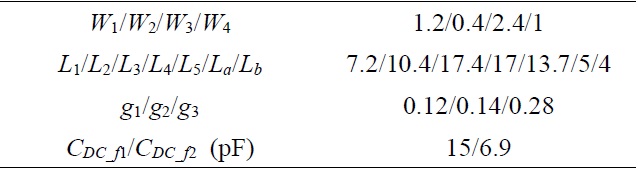
[Table 1.] Dimensions for fabricated filter I (unit=mm; refer to Fig. 1 for notation)

Dimensions for fabricated filter I (unit=mm; refer to Fig. 1 for notation)
1. Filter I: Tunable Center Frequencies
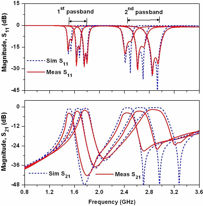
Fig. 5 shows the simulation and measurement results of filter I for several typical bias voltages. The measurement results agree well with the simulation results. The measurement results show that the first passband center frequency can be tuned from 1.48 to 1.8 GHz and the second passband center frequency can be tuned from 2.40 to 2.88 GHz.
The return loss is better than 12 dB in the overall tuning range of both passbands. The insertion loss varies from 1.99 to 4.4 dB at the first passband, whereas it varied 1.60 to 4.2 dB at the second passband. As the passbands are tuned towards lower frequencies, the insertion loss becomes higher. Because of decreasing bias voltages, the Q value of varactors becomes lower.
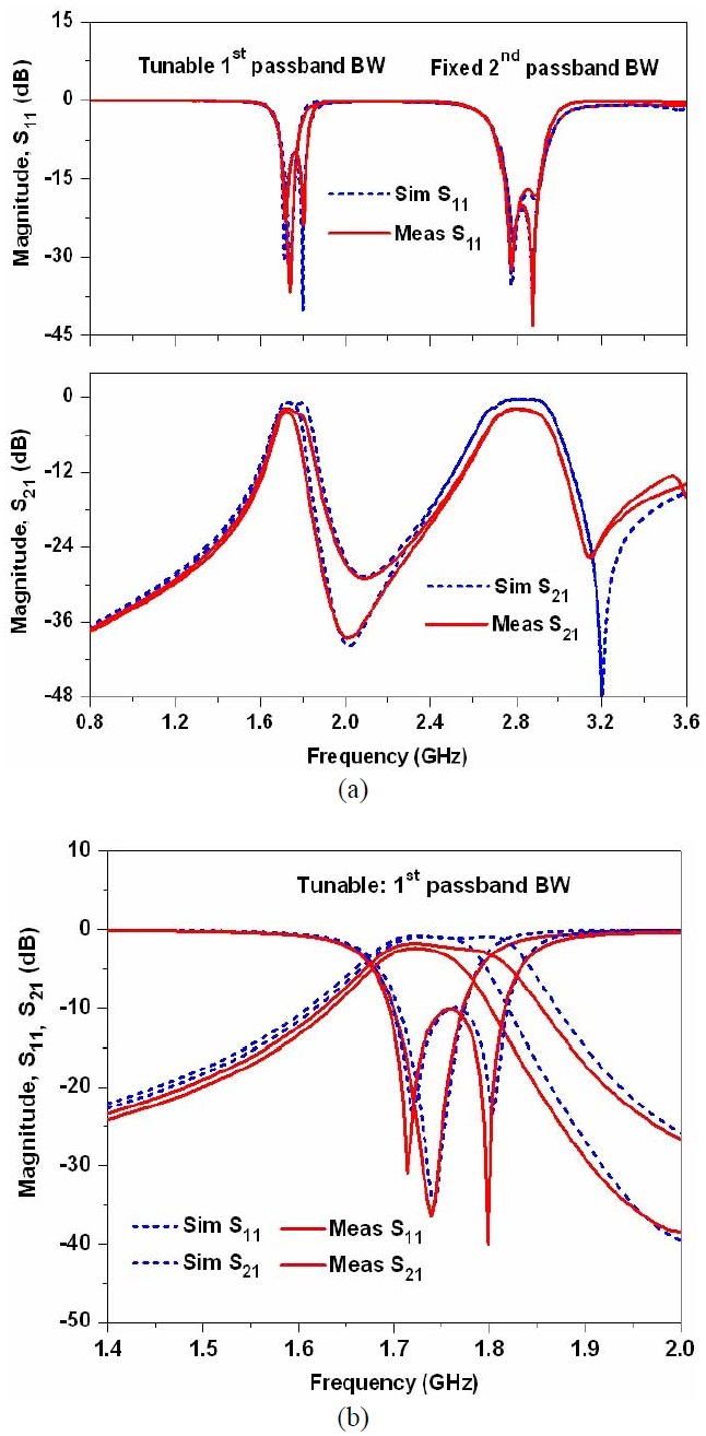
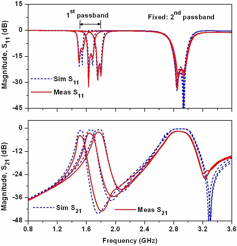
Fig. 6 shows the simulation and measurement results of filter I with the fixed second passband and tunable first passband center frequencies. The second passband center frequency is fixed at 2.88 GHz and the first passband center frequency is tuned from 1.48 to 1.8 GHz. The return loss is better than 12 dB over the entire tuning range of the first passband. The insertion loss varies from 1.99 to 4.42 dB.
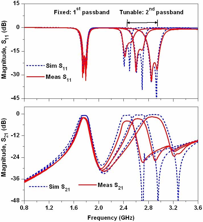
Fig. 7 shows the simulation and measurement results of filter I with the fixed first passband and tunable second passband center frequencies. The first passband center frequency is fixed at 1.74 GHz, and the second passband center frequency is tuned from 2.40 to 2.88 GHz with the return loss better than 12 dB over the entire tuning range.
The insertion loss varies from 1.64 to 4.2 dB. From these results, it is clear that the center frequencies of proposed filter can be tuned independently. However, the differences in insertion loss between the simulation and measurement results are due to the use of ideal capacitances in EM simulation.
2. Filter I: Tunable Bandwidths
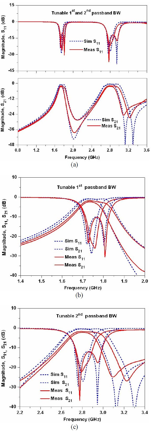
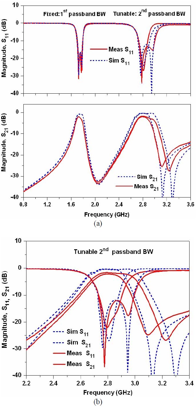
Fig. 8 shows the simulation and measurement results of filter I with both tunable passband bandwidths. As seen in this figure, the first passband’s 3-dB FBWs could be tuned from 5.76% to 8.55% at 1.74 GHz and the second passband’s 3-dB FBW variation was from 8.28% to 12.42% at a center frequency of 2.80 GHz.
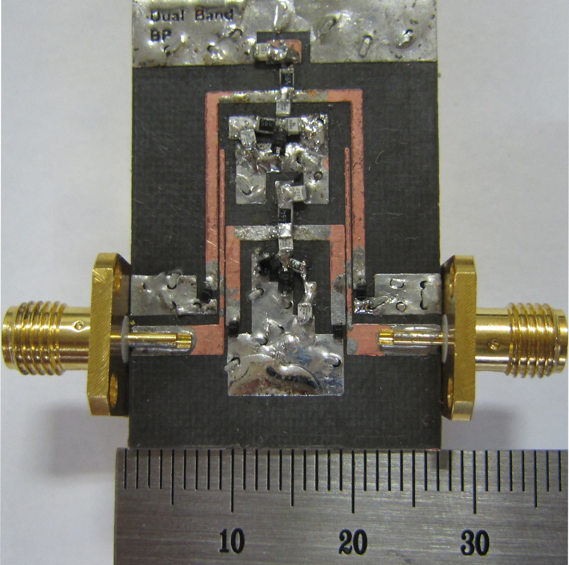
Figs. 9 and 10 show the simulation and measurement results for filter I, which independently verify the tunable 3-dB FBWs of the passbands. As seen in Fig. 9, the 3-dB FBW of the first passband is tunable with the fixed second passband bandwidth. Similarly, Fig. 10 shows the simulation and measurement results for the tunable 3-dB FBWs of the second passband with the fixed first passband bandwidth. A photograph of the fabricated filter I is shown in Fig. 11.
3. Filter Ⅱ: The Tunable Dual-Band Bandpass Filter with Harmonic Suppression
It can be observed from the simulation and measurement results in the previous section that the two passbands have several harmonics.
These harmonics are also tuned by varying the passband frequencies and must be suppressed for overall system performance.
A simple method of suppressing the harmonics is the introduction of a transmission zero at the harmonic frequency [15]. However, this method would be inefficient, because it can only suppress the harmonics around a specific frequency. Due to a broad range of variation in the harmonic frequency in the case of a tunable dual- band BPF, it is not possible to cancel harmonics sufficiently by a simple transmission zero circuit. The DGS of the microstrip line is implemented by making artificial defects on the ground plane; it provides band-rejection characteristics corresponding to the size and shape of defects on the ground plane. The DGS also provides an additional effective inductance in the transmission line, which enables the slow-wave factor of line to be increased. These band-rejection properties and the slow-wave effect of DGS have been applied in the design of various microwave circuits, including filters, dividers, and amplifiers [16,17].
In microwave circuit design, the band-rejection property of the DGS can also be utilized in the suppression of harmonics [13,17].
Fig. 12 shows the proposed configuration and photograph of fabricated harmonic suppressed tunable dual- band filter Ⅱ. In this structure, DGS is used at the input/output feeding lines for inducting coupling and acts as a broad band-rejection resonator to suppress the harmonics of filter I. The methods for finding the equivalent circuits of DGS are detailed in [16]. The physical parameters and component values of filter Ⅱ are shown in Table 2.
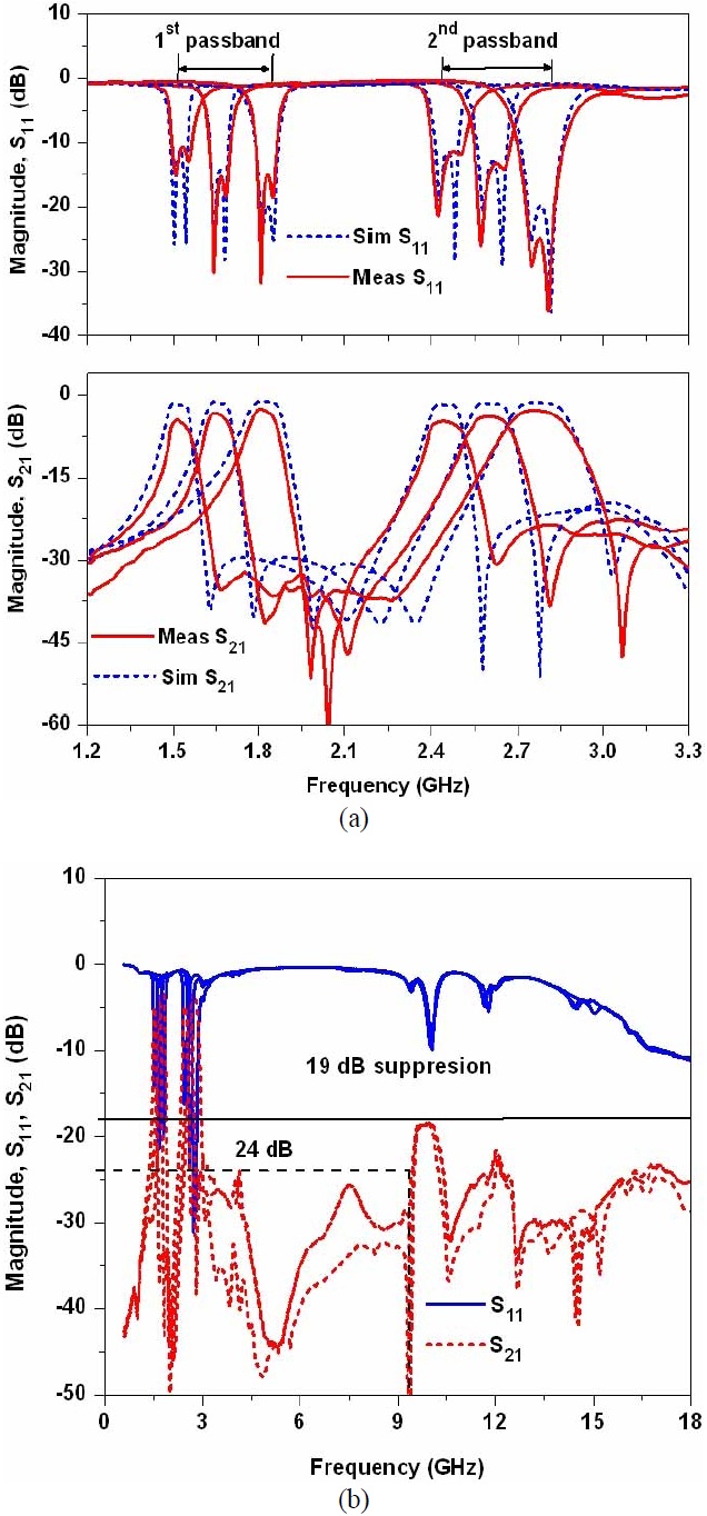
Fig. 13(a) shows the narrowband characteristics of the simulation and measurement results for filter Ⅱ. The passband frequencies are tuned with the help of the bias voltages of the varactor diodes. From the measurement results, the first passband frequency can be tuned from 1.5 to 1.8 GHz and the second passband frequency can be tuned from 2.45 to 2.80 GHz. The return loss is better than 11 dB over the entire tuning range of the passbands. The insertion loss varies from 3.02 to 4.8 dB at the first passband and 2.78 to 4.6 dB at the second passband. These measurement results for filter Ⅱ are almost similar to the filter I results in the previous section, except for the suppression of the harmonic characteristics.
[Table 2.] Dimensions for fabricated filter Ⅱ (unit=mm; refer to Fig. 12 for notation)
Dimensions for fabricated filter Ⅱ (unit=mm; refer to Fig. 12 for notation)
In order to verify the harmonic suppression characteristics of filter Ⅱ, the broadband harmonic suppression characteristics are shown in Fig. 13(b). The harmonic suppression characteristics for the fabricated filter Ⅱ are better than 19 dB up to 18 GHz over the entire tuning range of the passbands. This means that the proposed structure can suppress more than 10th order harmonics of the highest center frequencies of the first passbands due to the band-rejection characteristics of DGS. This confirmed that the proposed method can achieve broadband harmonic suppression without degrading any passbands performances. Performance comparisons of the proposed tunable filter with other tunable filters reported in the literature are summarized in Table 3. The proposed filter can provide dual-passbands with independently tunable center frequencies and bandwidths in addition to broadband harmonic rejection characteristics.
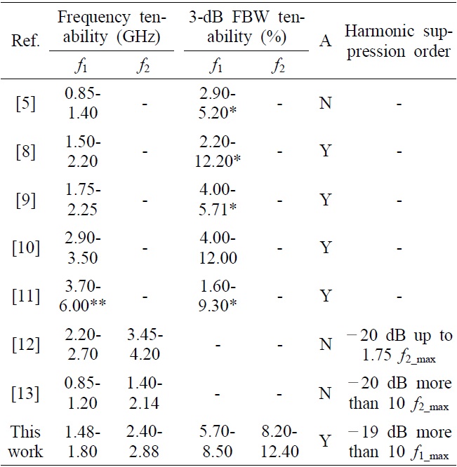
Performance comparison of tunable filter with independent control of center frequency and bandwidth
In this paper, the design of tunable dual-band BFPs with independently tunable center frequencies and bandwidths was demonstrated. The proposed structure is validated by both theoretical analysis and experiments. Defected ground structures were utilized to reject the harmonics. The experimental results are in good agreement with the theoretical predictions. These experimental results showed that the first passband can be tuned from 1.48 to 1.8 GHz with a 3-dB fractional bandwidth tunability of 5.76% to 8.55%, while the second passband can be tuned from 2.40 to 2.88 GHz with a 3-dB fractional bandwidth tunability of 8.25% to 12.42%. The proposed filter also offers switchable passband characteristics.
The proposed method can suppress more than 10th order harmonics of second passbands, thereby ensuring broad harmonic rejection characteristics without any degradation of the passband characteristics. The proposed filter topology is simple to implement and a good candidate for communication systems requiring multiband tunable filters with center frequency and bandwidth control. The proposed filter design method can be applied to selectable multimode or multiband applications that have different operating frequencies and bandwidths.