High-electron-mobility transistors (HEMTs) have been highlighted as essential high-frequency devices for various state-of-the-art microwave or millimeter-wave application systems, such as satellite communication, electronic warfare, radiometry, base stations, and smart weapons [1-3]. These systems require not only excellent radio frequency (RF) characteristics but also high-power performances for their specific applications [4]. The enhancement of power characteristics can be achieved by improving the current level or breakdown voltage of the HEMTs. A variety of methods have been used to increase the power performance of HEMTs these include the GaN/AlGaN material system [5,6], the gate-fieldplate technique [7,8], and the adoption of composite channel systems [9,10]. Most of these methods have focused on the enhancement of transistor power by increasing the breakdown voltage. These technologies, however, have some drawbacks, such as high cost and difficulty in material growth of the composite channel HEMTs, poor RF characteristics of the GaN HEMTs, and low electron mobility and large increase in the parasitic capacitances of the gate-field-plated HEMTs. As a consequence, in many application achieving a large current level by simply increasing the transistor gate_width (w) has been one of the most economic and practical methods in terms of circuit design and device fabrication.
A very long gate width or multi-finger gates are effective, but an increase in w gives rise to a large gate resistance (Rg), thereby causing degradation of noise characteristics [11] and the maximum frequency of oscillation (fmax) [12]. Therefore, it preferable to achieve a long effective gate width with no significant increase or even reduction in Rg. The use of a wide-head T-gate was reported [11] as an exemplary method for suppressing Rg; however, this technique has a limit in expanding the gate head because high source-to-drain channel resistance is unavoidable under increased source-drain spacing for accommodating a wide gate-head dimension; consequently, the structural instability of the T-gate increases in this structure. Even though studies [13-15] have documented the critical role of Rg in the high-frequency characteristics of HEMTs based on a small-signal- equivalent circuit model, there has been minimal investigation in reducing Rg in HEMTs with long gate_ widths or multi-finger gates. In this study, we investigated the multi-finger structures of the HEMTs affecting Rg and high-frequency characteristics. Because Rg is strongly influenced by a number of gate_fingers (N) and gate_widths (w) of the device structure, we examined the effects of all these parameters on Rg and the device characteristics by using various combinations of structural parameters for the 0.1-μm depletion-mode InGa- As/InAlAs metamorphic HEMT (MHEMT). To investigate the effects of N and w, 12 different gate peripheries were fabricated with various gate fingers (2, 4, and 6) and gate widths (25, 40, 50, and 70 μm). Except for the variations in N and w, we maintained the same epitaxial structure, gate length of 0.1-μm, and source-drain spacing of 2-μm for all fabricated devices, as described in the next section.
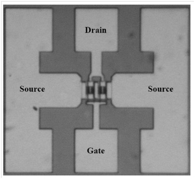
The MHEMT micrograph of the HEMT with four fingers is shown in Fig. 1.
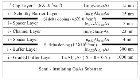
As shown in Fig. 2, the MHEMT epitaxial structure was grown by molecular beam epitaxy on a semi-insulating GaAs substrate. The structures consisted of the following layers from the bottom: a 1000-nm InxAl1-xAs linearly graded buffer layer with an indium mole fraction, x, linearly graded from 0 to 0.5; a 300-nm undoped In0.52Al0.48As buffer layer; a silicon delta-doped plane (1.3×10¹²/cm2), a 4-nm undoped In0.52Al0.48As spacer layer; a 23-nm undoped In0.53Ga0.47As channel layer; a 3-nm undoped In0.52Al0.48As spacer layer; a silicon delta- doped plane (4.5×10¹²/cm2); a 15-nm undoped In0.52 Al0.48As Schottky barrier layer; and a 15-nm n-type In0.53Ga0.47As cap layer (6×10¹⁸/cm3). The grown epitaxial layer showed a two-dimensional electron carrier density (ns) of about 3.5×10¹²/cm2 and a Hall mobility of about 9,700 cm2/Vsec at room temperature.
To fabricate the MHEMTs, we first isolated active areas by using mesa etching with an etchant of phosphoric acid/H2O2/H2O (1:1:60) to reduce the thickness to 200-nm. AuGe/Ni/Au (140/30/160 nm) ohmic metallization showed a specific contact resistance of about 5×10―7 Ω-cm2 after rapid thermal annealing at 320℃ for 60 seconds in a vacuum. An electron beam lithography system (EBPG-4HR, Leica Microsystems Ltd., Buffalo Grove, IL, USA) was used to perform 0.1-μm T-shaped gate patterning upon completion gate_recess, gate metallization was performed by evaporating Ti/Au (50/400 nm) followed by metal lift-off. The MHEMTs were passivated with the Si3N4 films (80 nm). Finally, a Ti/Au (30/700 nm) air-bridge interconnection was made to connect the source pad.
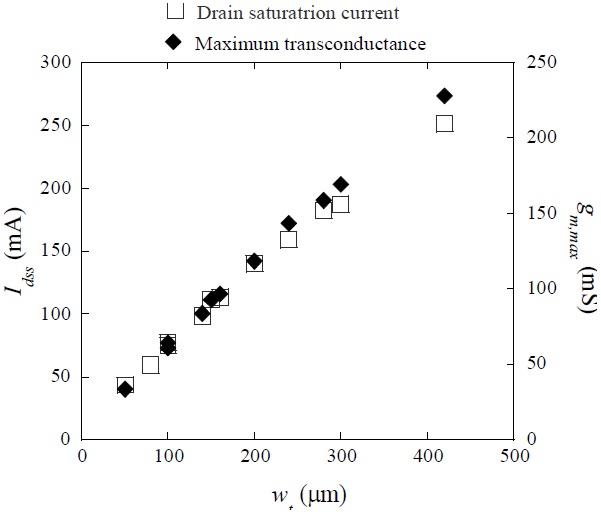
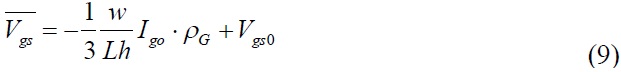
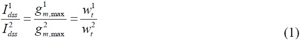
The DC characteristics of each MHEMT were measured in an HP 4156 DC parameter analyzer. Drain current (Ids) versus gate voltage (Vgs) and transfer characteristics of the MHEMTs (at a drain voltage [Vds] of 1.2 V) were measured at various N and w values. With the total gate width (wt), the saturation drain current (Idss) and maximum transconductance (gm,max) were linearly increased at constant slopes of about 0.58 mA/μm and 0.57 mS/μm, respectively, as shown in Fig. 3. The wt is hereafter defined as “total gate width” and given by the product of N and w. The scaling rules for these parameters are then simply expressed as:
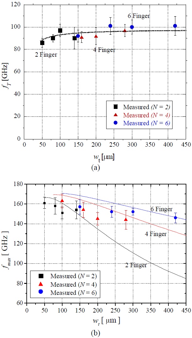
High-frequency characteristics of the fabricated MHEMTs were measured in the frequency range of 0.5 to 50 GHz using an HP8510C network parameter analyzer (Agilent Technologies, Palo Alto, CA, USA). Cut-off frequency (fT ) and fmax were determined by extrapolating the h21 and U gain curves, respectively, at a slope of 6 dB/octave. The DC and RF data were measured from each gate type of the MHEMTs at six different dies a 2.5×2.5 cm2 specimen. The average fT and fmax from the MHEMTs with 12 different gate types measured from six different dies were plotted respectively in Fig. 4 with their standard deviations (1σ). The fT increased slightly in a small wt region and was saturated to a frequency of about 100 GHz; on the other hand, the fmax decreased continuously with the wt in our whole experimental range of wt, and the reduction ratio was a function of N.
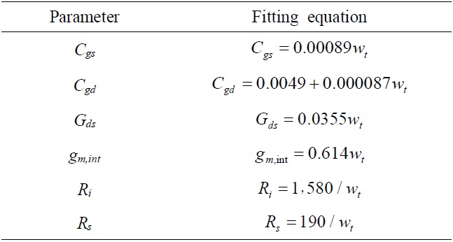
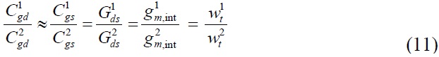
To examine the effects of N and wt on the small-signal parameters directly affecting fT and fmax, all the parameters shown in Eqs. (2) and (3) [16,17] were extracted from the fabricated MHEMTs by the Dambrine method [18] and curve-fitted to simple functions of wt. As shown in Table 1, gate-to-source capacitance (Cgs), gate-to-drain capacitance (Cgd), drain conductance (Gds), and intrinsic transconductance (gm,int) were proportional to wt.
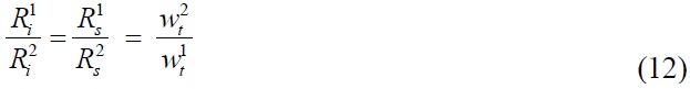
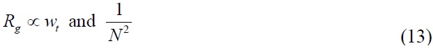
However, intrinsic resistance (Ri) and source resistance (Rs) were inversely proportional to wt. All these parameters were functions of wt. But were not functions of N; however, one exception was Rg, which was a function of both wt and N.
The relationships of the fitted parameters with wt can be explained as follows. Cgs is a function of Cgso which is gate-to-source capacitance per unit gate width, and therefore is expressed as

where Cgso is about 0.00089 pF/μm in our case. In the case of the Cgd, y-axis intercepts should also be considered. A non-zero Cgd at zero wt can be formed between the gate bus line and drain pad and this parasitic capacitance, in fact, has been observed in earlier studies [13,19,20]. In our case, the y-axis intercept of Cgd was about 0.0049 pF, and the proportionality constant was about 0.000087 pF/μm. The linear relationship of Gds with wt can be understood such that the total sourcedrain conductance is given by (dIds/dVds per unit gate width)×wt, and the corresponding proportionality constant was about 0.0355 mS/μm in our case. Rs and Ri were inversely proportional to wt and curve-fitted in the same way with the proportionality constants of about 190 and about 1,580 Ω?μm, respectively. The linear increase of gm,int with wt can be explained by the linear scaling rule of gm,ext with wt, as shown in Eq. (1); the proportionality constant was about 0.614 mS/μm.
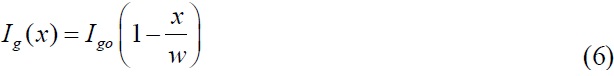
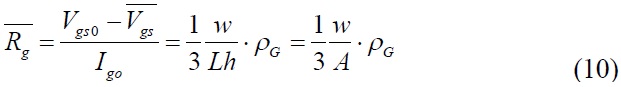
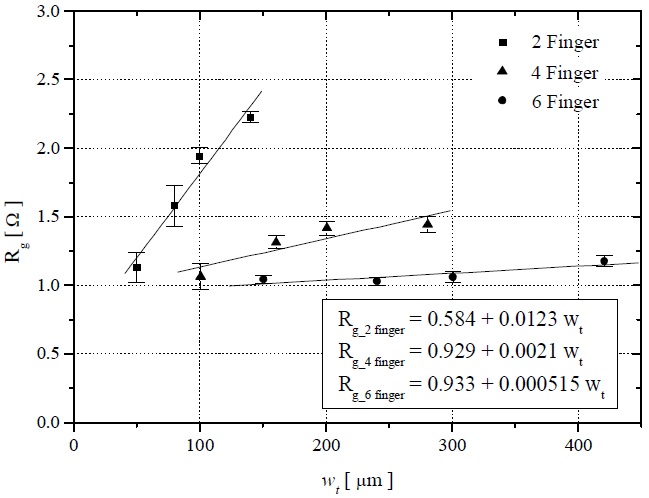
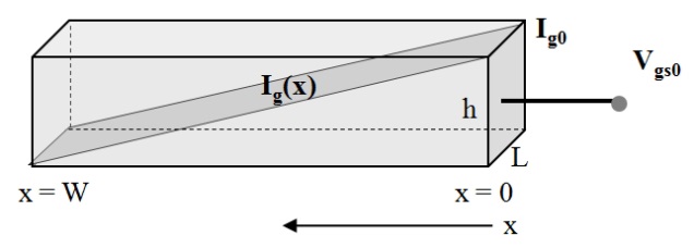
Rg is a function of both N and wt, as shown in Fig. 5, and can be expressed as Eq. (5) where ρG is the resistivity of the gate metal, and A is the cross-sectional area of the gate. Ro is the y-axis intercept obtained by linear curve fitting. This relationship can be obtained by assuming the gradual (linear) reduction in gate current (Ig) density as the open end is approached, as illustrated in Fig. 6, and an essentially uniform displacement current fed from the bottom of the gate to the channel region of the HEMTs [21]. In the open-ended gate structure shown in Fig. 6, Ig and the infinitesimal change of Vgs (δVgs) over δx are given by Eqs. (6) and (7),
where L and h are gate-length and gate-height, respectively. The minus sign in Eq. (7) indicates that gate voltage decreases with increasing x. At x=0, Vgs is equal to Vgs0, gate terminal voltage. Gate voltage Vgs (x) is obtained by integrating Eq. (7) with the boundary condition at x=0.
The average gate voltage is equal to the integral of Vgs (x) from x=0 to W and then divided by W. After carrying out the definition, we find the average value to be
The average intrinsic gate resistance inside the gate electrode region from x=0 to w is then given by:
Investigations have focused on Ro, Rg when w approaches zero [21,22]; however, the model for Ro, is still not fully understood. In our case, the y-axis intercepts of the MHEMTs (N=2, 4, and 6) range from about 0.6 to 0.9 Ω, with the corresponding proportionality constants of about 0.0123, 0.0021, and 0.000515 Ω/μm, respectively, as shown in Fig. 4. Therefore, the scaling rules of the small-signal parameters can be summarized as follows:
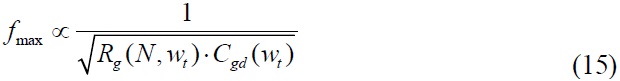
fT and fmax can be calculated by substituting each small-signal parameter of Eqs. (2) and (3) with the curve-fitting equations in Table 1. The calculated results are plotted in Fig. 4 with measurements at each N and wt. Good agreement was obtained from the calculated fT and fmax with the measured data over the entire range of measured wt. Some discrepancies between the measurements and the calculations are due to the errors associated with the device process in pattern lithography. Because gm and Cgs are both proportional to wt, as shown in Eq. (2), fT is not a function of wt. From our calculations contained in Fig. 3, fT showed an almost constant frequency of about 100 GHz above a wt of about 100-μm. Below this wt fT a slight increase with wt owing to the y-axis intercept effect of Cgd, as observed in many earlier studies [23,24]. Since fmax is a strong function of Rg as shown in Eq. (3), it is affected by both N and wt. If we assume that Gds is negligible (ideal case without channel length modulation), Eq. (3) is simply expressed as [25]:
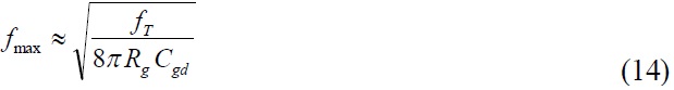
Because fT is almost constant, we therefore obtain:
Eq. (15) shows that a careful combination of N and wt is required to achieve a maximum fmax in a given device technology. Obviously, a greater wt produces a higher fmax; however, to increase the number of gate-fingers by reducing the unit gate width is more efficient than to simply increase the single-gate_width in order to maximize fmax at a given wt.
We investigated the effects of N and w on the RF characteristics of 0.1-μm depletion-mode multi-finger MHEMTs and their small-signal parameters. Cgs, Cgd, Gds, and gm,int were all proportional to wt; however, Ri and Rs were inversely proportional to wt. Rg was proportional to both wt and 1/N2. fT and fmax were calculated by using the small-signal models and curve-fitting equations from each extracted small-signal parameters. The calculations showed good agreements with the measurements, and the results demonstrated that a greater wt produces a higher fmax; however, to maximize fmax at a given wt, increasing the number of gate_fingers is more efficient than increasing the single-gate width. On the other hand, fT showed an almost independent relationship with wt. To our knowledge, this is the first successful demonstration of multi-finger gate-width scaling effects (individual effect of N and wt) on HEMT devices operating at millimeter-wave frequencies.