The artificial magnetic conductor (AMC) surface, also called the meta-surface, high-impedance surface, or reactive impedance surface, has been widely used as an artificial ground plane or reflector to enhance performance of many different antenna types while achieving profile miniaturization [1,2]. An AMC works as a perfect magnetic conductor (PMC) at resonant frequencies with the 0° phase of the reflected wave when illuminated by a normally incident plane wave. Its bandwidth is defined as the frequency range over which the phase of the reflection coefficient is between ±90° [2].
In many applications, an antenna works at different frequencies simultaneously [3-10]; consequently, the AMC requires multi-band operation that can match with the antenna’s working frequencies. Several different AMC structures have been developed for dual-band operation, including double bowties [11], concentric squares [12], or hexagonal patches [13] on a unit cell, in order to achieve dual-band characteristics. In addition, a mushroomtype cell loaded with symmetric meandered slots has been applied as a dual-band meta-surface [14]. However, the lack of miniaturization means that most of these AMCs have a large unit-cell size compared with the effective wavelength. A genetic algorithm has been used to develop multiband AMC surface designs by simultaneously optimizing the geometry and size of the unit cell [15]; however, these frequency bands are not easy to adjust independently. Dual-frequency operation can be achieved using two layers of a square patch with varactor diodes [16] or double patches incorporated with lumped capacitors [17]. However, both of these techniques increase the complexity and cost of the AMC.
In this paper, we describe a miniaturized dual-band AMC structure that allows easy control of the second/first resonant frequency ratio; this is achieved by inserting four slots into the metallic patch of a unit cell. We demonstrated the dual-band characteristics by fabricating and analyzing a wideband monopole suspended over the proposed AMC surface. The antenna over the AMC surface has measured impedance bandwidths of 2.37-2.59 GHz and 4.28-5.62 GHz for a ―10 dB reflection coefficient and unidirectional radiation patterns. We used the ANSYS- Ansoft high-frequency structure simulator (HFSS) in this study.
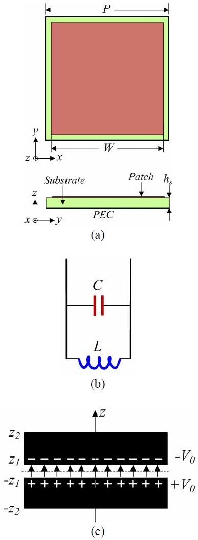
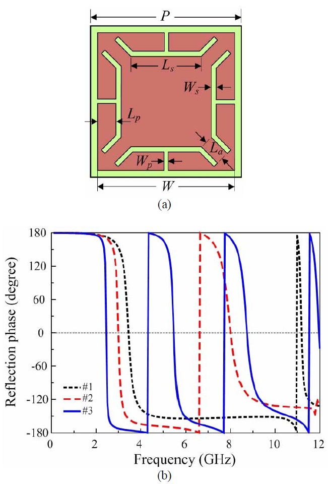
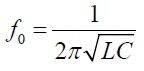
Fig. 1 shows the unit cell of the initial AMC design, which is a two-dimensional square metal patch structure printed periodically on a grounded substrate. The initial design, denoted as #1, was first proposed and analyzed in [2]. In the present paper, we undertake a brief inves tigation of its features. In the simulations, the unit cell was excited by a single-mode wave port at the top and subjected to a periodic boundary condition along the x- and y-axes [18]. The resulting structure can be considered to behave as a parallel LC circuit in Fig. 1(b), where the edge coupling of the square patch functions as a shunt capacitor (C), while the short-circuited dielectric- loaded transmission line is modeled as a shunt inductor (L). Therefore, the resonant frequency of the circuit can be expressed as follows:
where C=leffC0, with leff as the effective length of the square patch and C0 as the existence capacitor per unit length, determined based on the coplanar stripline modeling shown in Fig. 1(c). The variation in the patch size and the gap separation influences L, whereas the substrate thickness and permittivity mainly affect C; both parameters can be used to control the resonant frequency. The calculations of L and C have been detailed in [2].
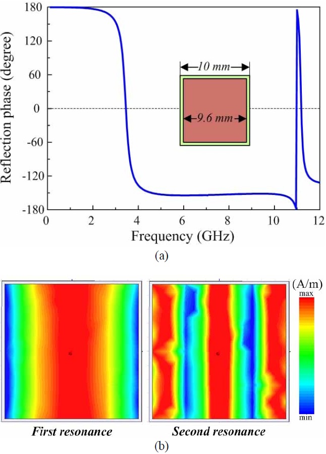
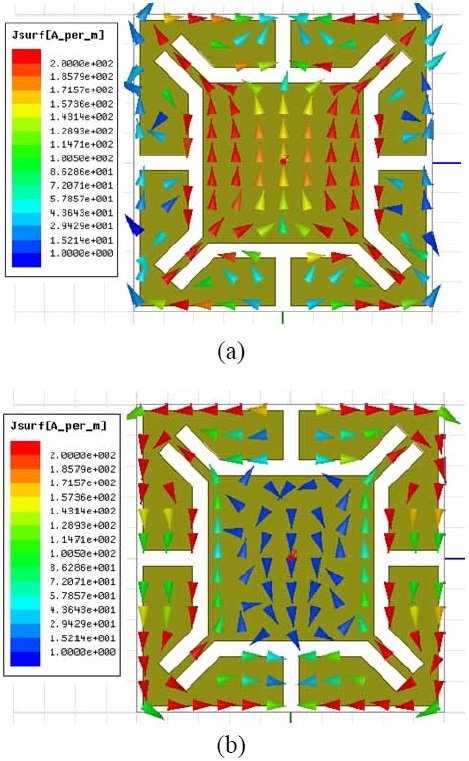
Previous research on this subject was concerned only with the primary resonant frequency for various design parameters of the unit cell. However, the use of the simulator to investigate the structure shown in Fig. 1 reveals the existence of higher resonant frequencies, as shown in Fig. 2(a), which shows the simulated reflection phase of the initial AMC. Here, a unit cell of the initial design with a 9.6 mm2 square metallic patch was built on a grounded 10×10 mm RT/duroid 6010 (Rogers Corp., Roger, CT, USA) substrate having εr=10.2, tan δ=0.0023, and hs=1.27 mm. Fig. 2(a) shows that the resulting structure had first and second resonant frequencies of 3.44 and 11.18 GHz, respectively. This result is depicted in Fig. 2(b), which shows the simulated surface current (Jsur) distribution on the patch at the first and second resonant frequencies. Standing waves appeared in the patch at both frequencies. Along the incident E-field direction, 1/2 and 3/2 periods of the Jsur magnitude appeared at the first and second resonant frequencies, respectively. The patch size was therefore approximately equal to 0.5 λeff for the first resonance and 1.5 λeff for the second resonance, where λeff is the effective wavelength. This behavior is nearly identical to the resonance behavior of the square patch microstrip antenna that was investigated theoretically using several methods and verified experimentally in [19].
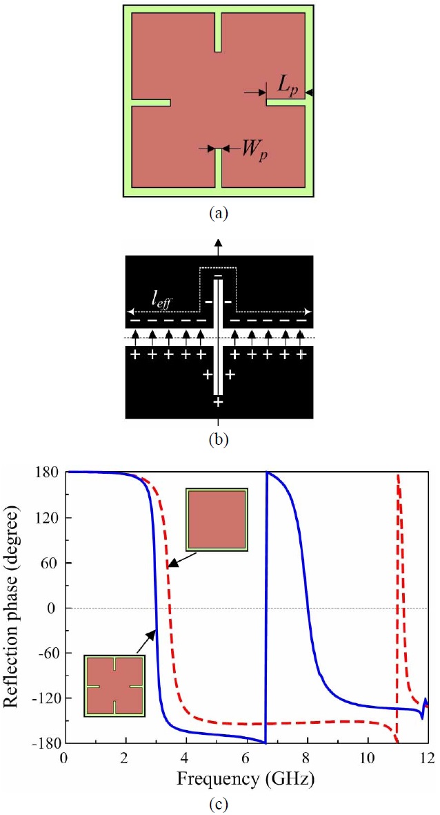
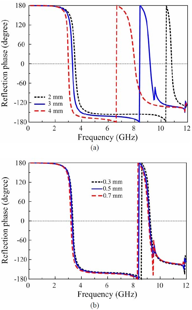
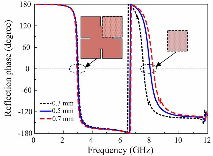
The capacitor (C) in the equivalent circuit of #1 can be adjusted simply by making suitable changes in the geometry of the periodic metallic sheet; consequently, the corresponding resonant frequencies can be modified and controlled [15]. Accordingly, the four slots are symmetrically inserted into the metallic patch of the initial AMC in Fig. 3(a), denoted as #2, to decrease the resonant frequencies for the same volume. Each slot was designed with a length and width of Lp and Wp, respectively. Fig. 3(b) shows that the effective length (leff) of the square patch increased significantly after the insertion of the slots, whereas C0 was hardly influenced by a Wp of less than W/10. Therefore, the capacitance (C=leffC0) increased, and consequently, the resonant frequencies decreased. This result can be observed definitively in Fig. 3(c), which shows the simulated reflection phases for #1 and #2. Each slot in #2 was designed with Lp=4 mm and Wp=0.5 mm. Fig. 3(c) shows that the first and second resonance frequencies of #2 were 3 and 8 GHz, respectively; these are considerably lower than the corresponding values for #1. We realized that the variation in the slot width (Wp) slightly affected the reduction in resonant frequency because leff depends only on the slot length (Lp). This result is also evident from Fig. 4, which shows that the variations in the slot length (Lp) and width (Wp) affected the reflection phase of #2. The first and second resonant frequencies decreased significantly as Lp increased in Fig. 4(a) but were unaffected by the changes in Wp in Fig. 4(b). However, the effect of Wp was not the same for all values of Lp. For example, when Wp was varied, the resonant frequencies of #2 barely changed for Lp values smaller than 3 mm. However, for Lp values greater than 3 mm, the first resonant frequency was only slightly affected, while the second resonant frequency increased significantly. We can understand that for a large Lp value, the first resonance is generated by the entire patch, whereas the second resonance occurs because of the four smaller squares located in the corners of the patch, as shown in Fig. 5. This concept has been proposed and investigated in [15].
We further reduced and controlled the resonance frequencies by modifying the slots in the metallic patch of #2 into T-shapes, denoted as #3, as shown in Fig. 6(a). The #3 design is the proposed AMC structure optimized to obtain the first and second resonance at approximately 2.45 and 5.5 GHz, respectively. The optimized design parameters of each slot are as follows: Lp=1.6 mm, Wp=0.5 mm, Ls=5 mm, Ws=0.5 mm, and La=1.8 mm. The features of the proposed structure were almost the same as those of #2, but it yielded considerably lower resonance frequencies. This result can be observed in Fig. 6(c), which shows the simulated reflection phases for all steps of the AMC design process. Here, #2 was chosen with Wp=0.5 mm and Lp=4 mm. We can see that the resonant frequencies of #2 decreased significantly compared with those of #1, and its second/first resonant frequency ratio was approximately 2.67. The #3 design yielded considerably lower resonant frequencies than #2; its first and second resonance frequencies were 2.45 and 5.5 GHz, respectively, and the frequency ratio was approximately 2.24. The simulation shows that the proposed AMC yielded bandwidths of 2.42-2.48 GHz and 5.38-5.57 GHz for the ±90° reflection phase at its first and second resonance frequencies, respectively. These results indicate that miniaturization of the AMC unit cell was achieved by the insertion of slots into the metallic patch.
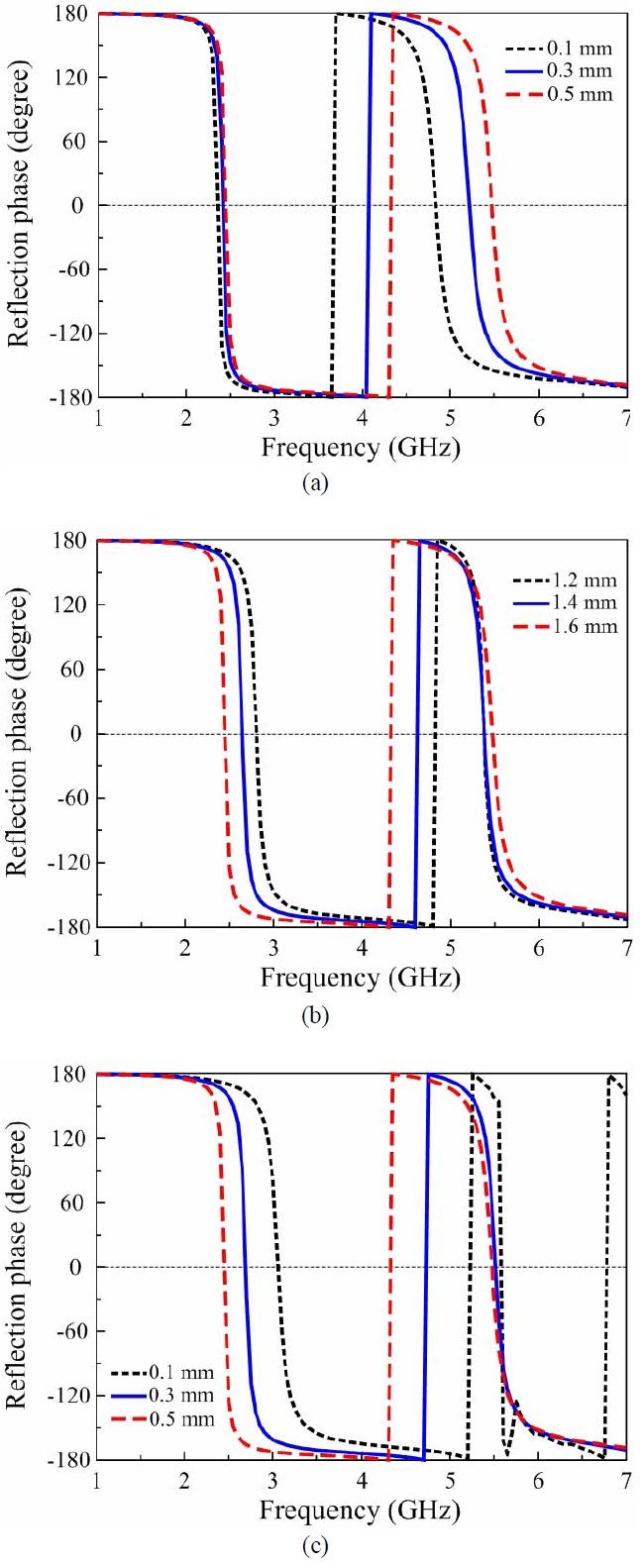
Fig. 7 shows the simulated current distribution on the metallic patch surface of the #3 AMC at the first and second resonant frequencies. The first resonance is generated by the entire patch, whereas the second resonance is generated by the small section in the corners of the patch. The proposed AMC structure provides easy control over the second/first resonant frequency ratio because it retains the features of #2 with large Lp and has a coupling between the angled parts (La) of the two neighboring slots in the metallic patch. This feature is clearly observed in Fig. 8, which shows the simulated reflection phase for the different design parameters of the metallic patch of a unit cell that strongly affect the second/first resonant frequency ratio. In the simulation, one parameter is varied while the other parameters are fixed, similar to the case of #3. Fig. 8(a) shows that an increase in Wp from 0.1 to 0.5 mm in 0.2-mm steps caused almost no change in the first resonant frequency, while the second resonant frequency increased significantly; consequently, the second/first resonant frequency ratio increased. An increase in Lp from 1.2 to 1.6 mm in 0.2-mm steps decreased the first resonant frequency, while the second resonance frequency remained almost the same; consequently, the second/first resonant frequency ratio again increased in Fig. 8(b). Fig. 8(c) shows that a stepwise increment of 0.2 mm in Ws from 0.1 to 0.5 mm decreased the first resonant frequency, while the second one barely changed; consequently, the second/first resonant frequency ratio again increased. The HFSS simulations show that a metallic patch having dimensions of W=9.6 mm, Lp=1.4 mm, Wp=0.1 mm, Ls=4 mm, Ws=0.1 mm, and La=1.8 mm yielded the minimum second/first resonant frequency ratio of 1.5. The metallic patch without a slot, which was labeled #1, yielded the maximum second/first resonant frequency ratio of 3.26. Therefore, the proposed AMC can be easily applied to dual-band operation by using its first and second resonance frequencies. In addition, the HFSS simulations show that the minimum frequency of 1.6 GHz in the first resonance can be achieved with W=9.6 mm, Lp=4.5 mm, Wp=0.1 mm, Ls=0.2 mm, Ws=0.1 mm, and La=6.4 mm. When compared with #1, which yielded the first resonant frequency of 3.44 GHz, the miniaturization factor is greater than two.
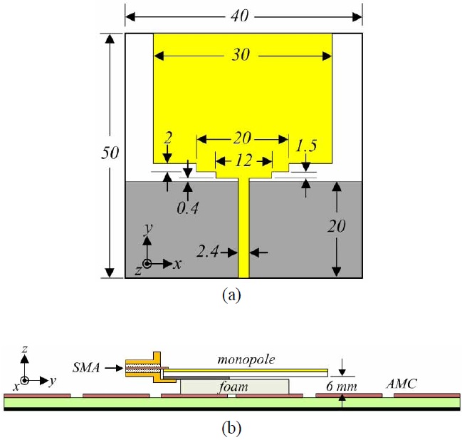
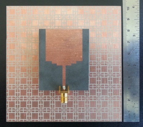
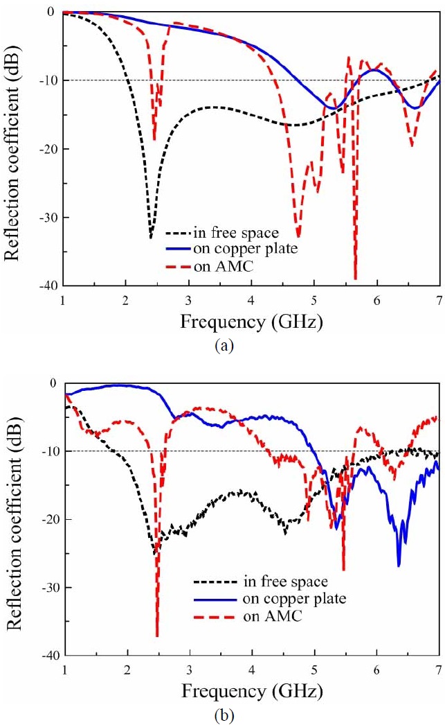
Both a perfect electrical conductor (PEC) and a PMC surface are known to have a strong coupling with the antennas above them [2]. When the antenna is placed in close proximity and parallel to a PEC, its impedance matching is rather difficult. In contrast, the impedance matching of the antenna in close proximity to a PMC appears to be easier. Accordingly, the antenna system was designed to prove that the proposed AMC worked as a PMC at the resonance frequencies. We confirmed the features of the proposed AMC shown in Fig. 6 by designing, fabricating, and measuring a dual-band antenna (Fig. 9). A 10×10 cell array of #3 described in the previous section was chosen to form an AMC surface with overall size of 100 mm×100 mm×1.27 mm. A wideband monopole antenna was suspended 6 mm above the AMC using ROHACELL structural foam (Evonik Industries, Essen, Germany) having εr=1.07 and tan δ =0.0006. A wideband monopole that was fed by a 50-Ω microstrip line was fabricated on both sides of an RT/duroid 5880 (Rogers Corp.) substrate having εr =2.2, tan δ=0.0009, and thickness=0.7874 mm. An Agilent N5230A network analyzer and a 3.5-mm coaxial calibration standard GCS35M were used to conduct measurements on the prototype (Fig. 10). The monopole antenna was tested in free space and over a 100 mm×100 mm copper plate and AMC surface at a height of 6 mm. Fig. 11 shows the simulated and measured reflection coefficients of a monopole with different reflectors and shows a good agreement between the two. In free space, the antenna yielded a measured impedance matching bandwidth of 1.97-6.34 GHz for the ―10 dB reflection coefficient, while the simulated bandwidth was 1.9-6.8 GHz. For the antenna over the copper plate, both simulations and measurements showed that the antenna did not match well in the region near the 2.4 GHz but yielded a good match around 6 GHz. The antenna over the AMC yielded measured impedance bandwidths of 2.37-2.59 GHz and 4.28-5.62 GHz, while the simulated bandwidths were 2.40-2.58 GHz and 4.37-5.50 GHz. The first and second bands of the antenna system verified the dual-band capability of the proposed AMC. The impedance bandwidth became narrower after loading the AMC because the bandwidth of the antenna system depended on the operation bandwidth of the AMC.
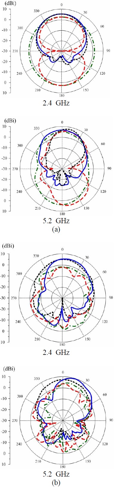
The radiation patterns were measured in a full anechoic chamber of dimensions 15.2 m×7.9 m×7.9 m. Fig. 12 shows the simulated and measured radiation patterns of the monopole antenna in free space and over the AMC surface at 2.45 and 5.2 GHz. The measurements agreed rather closely with the simulations. When compared with the antenna in free space, the gain of the antenna over the AMC surface increased in the forward direction by approximately 6 and 4 dB at the lower and upper frequencies, respectively. The antenna over the AMC yielded back-radiation reductions of 15 and 20 dB at 2.45 and 5.2 GHz, respectively, when compared with the antenna in free space. The radiation patterns at the upper frequency were not quite symmetric because of the monopole antenna’s geometry. Additionally, the ripples in the measured radiation patterns could be attributed to the effects of the foam rack and the tape used to fix the antenna into the measurement setup. These results indicate that the monopole over the AMC surface yielded a unidirectional radiation pattern with high front- to-back ratio in both bands.
A miniaturized AMC that uses the first and second resonance frequencies was introduced and tested for dual- band operation. We achieved the desired miniaturization and easy control of the second/first resonant frequency ratio by inserting four slots in a symmetrical fashion into the metallic patch of the AMC unit cell. We demonstrated the dual-band capability of the proposed AMC structure by suspending a wideband monopole over an AMC surface with resonance frequencies of approximately 2.45 and 5.2 GHz. The controllable frequency ratio, ease of fabrication, and miniaturized size of the proposed AMC structure support its potential use in dual-band wireless communication.