InGaN/GaN-based light-emitting diodes (LEDs) have attracted considerable interest because of their various industrial application in general lighting, backlight units in liquid crystal displays (LCD), full-color displays, and automotive head lamps [1-7]. Nowadays, the application of GaN LEDs has been extended to general lighting, which requires high-brightness and high-power operation. For high-brightness and high-power applications of solid-state general lighting, LEDs have to be operated at a high current density. However, in spite of significant improvements in its performance, the use of GaN-based LEDs is still seriously limited by the reduction in the external quantum efficiency (EQE) under high-injection-current-density conditions [8]. This well-known phenomenon is referred to as efficiency droop. Over the past years, several different suggestions regarding the mechanism of efficiency droop have been reported, including carrier leakage out of the multi-quantum well (MQW) active region [9,10], Auger nonradiative recombination [11], junction heating [12], the dislocation density [13], non-uniform distribution of holes [14], polarization fields [15] and the quantum-confined Stark effect (QCSE) [16]. Nevertheless, the major origin of the efficiency droop behavior is still not completely understood. For this reason, many approaches have been suggested to increase EQE and mitigate efficiency droop in recent years. Among them, for the GaN-based blue LEDs, it is notable that not only the polarization field in MQWs but also low injection and transport of holes are believed to be the main factors of the efficiency droop and the degradation in EQE. Conventionally, the strong piezoelectric and spontaneous polarization due to large lattice mismatch between InGaN well and GaN barrier layers cause an internal electric field perpendicular to the plane of the well layer, resulting in poor overlap between electron and hole wavefunctions in the well [17]. These effects give rise to decreased internal quantum efficiency (IQE). Furthermore, a p-type AlGaN electron blocking layer (EBL) is usually used between the p-type GaN layer and the active region to alleviate the electron leakage and to improve the device efficiency [18,19]. The EBL has played an important role in effectively confining electrons in the active region because the large conduction band offset between the last GaN barrier and the AlGaN layer is beneficial in preventing electron leakage out of quantum wells. However, it has been reported that a large polarization field in AlGaN EBL can reduce the effective barrier height for electrons [20]. On the other hand, the downward band-bending induced by the polarization field and the valence band offset at the interface of the last barrier of the MQWs and the AlGaN layer might act as a potential barrier for holes [21,22]. Therefore, the polarization-matched quarternary AlGaInN and InGaN quantum barriers have been suggested to reduce the polarization field in the active region and have been experimentally demonstrated to enhance the light-output power and to reduce the efficiency droop of LEDs [23,24]. It has been also reported that p-AlGaInN and p-AlInN EBL in LED structures can prevent carrier leakage over the EBL [25,26].
In this paper, in order to solve the above mentioned problem, we propose and investigate the effect of GaN/ graded-composition AlGaInN/GaN as quantum barriers in the active region on the performance of GaN-based vertical LED in comparison with those of conventional GaN quantum barriers. The inserted graded-composition AlGaInN barriers were used to reduce polarization effects between quantum well and barrier layer so that the carrier distribution and radiative recombination rate were improved, and thereby efficiency droop was alleviated. We use the Simulator of Light Emitters based on Nitride Semiconductors (SiLENSe) and the Spreading of Current in Light Emitting Diodes (SpecLED) programs to analyze enhancement of the device performance [27].
II. DEVICE STRUCTURE AND PARAMETERS
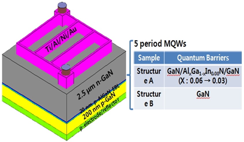
As shown in Fig. 1, the vertical LED structures for the numerical analysis were composed of a 2.5-μm-thick n-type GaN (n-doping = 5 × 1018 cm-3). The MQW active region consisted of five 3-nm-thick undoped In0.2Ga0.8N QWs separated by 12-nm-thick barrier layers with a 3×1018 cm-3 donor (Si) concentration. On top of the active region were a 20-nm-thick p-type Al0.15Ga0.85N EBL and a 0.2-μm-thick p-GaN (p-doping = 1.2 × 1018 cm-3 for both layers) cap layer. For a comparative study, two LED structures were assumed. The schematic diagrams of the LED structures with two different types of quantum barriers are shown in Fig. 1. In order to reduce the polarization effect of the
original LED structure with conventional GaN barriers, 8-nm-thick graded-composition AlGaInN layers are sandwiched by 2-nm-thick GaN barriers and are proposed to replace the conventional GaN barrier. The Al composition (x) of the graded-composition AlXGa1-XIn0.08N was gradually decreased from 0.06 to 0.03. The VLED with conventional GaN barriers and that with GaN/graded-composition AlGaInN/GaN barriers are referred to as structure A and structure B, respectively. The band offset ratio, ΔEC/ΔEV = 0.7/0.3, serves as a default parameter in the simulation. All the calculations are carried out with the threading dislocation density of 108 cm-2. The operating temperature is assumed to be 300 K. To simplify the simulation, the light extraction efficiency is assumed to be 0.7. The electron and the hole mobilities were assumed to be 150 cm2/Vs and 10 cm2/Vs, respectively. The area of the device geometry was 1 × 1 mm2. Other material parameters used in the simulation can be found in Ref. 28. For this simulation, the light-output power versus the current and the current versus the voltage (L-I-V) characteristics, the electroluminescence (EL) and internal quantum efficiency (IQE) were investigated by using the SimuLED package, which provides a coupled 3D analysis of the electrical, thermal, and optical processes.
The basic equations used for this study are Poisson’s equation and the current-continuity equations for electrons and holes, as represented by the following equations [29]:

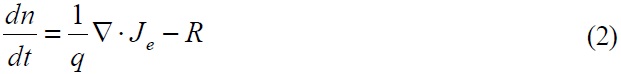
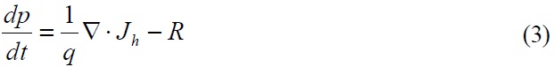
where ψ is the electric potential, n is the electron density, p is the hole density, Je and Jh are the current densities for electrons and holes, respectively, and R is a recombination term. In Eq. (1), ND and NA represent the ionized donor concentration and ionized acceptor concentration, respectively. In the simulation, the recombination term R in Eqs. (2), (3) and (4) was represented as follows:

where Rsp, RSRH, and RAug are the spontaneous emission recombination, the Shockley-Read-Hall nonradiative recombination, and the Auger recombination, respectively. Also, the internal quantum efficiency (ηint) was given by
The electron and the hole current densities are related to the fluxes as jn = -q · jn and jp = +q · jp. In turn, the carrier fluxes depend generally on the gradients of the quasi- Fermi levels as
where μn and μp are the electron and the hole mobilities, respectively. Moreover, commonly-accepted parameters are used in the simulations, including a Shockley-Read-Hall (SRH) recombination lifetime of 50 ns and an Auger recombination coefficient of 1×10-31 cm6s-1 [30] at the interfaces between the InGaN well and GaN barrier in the active region.
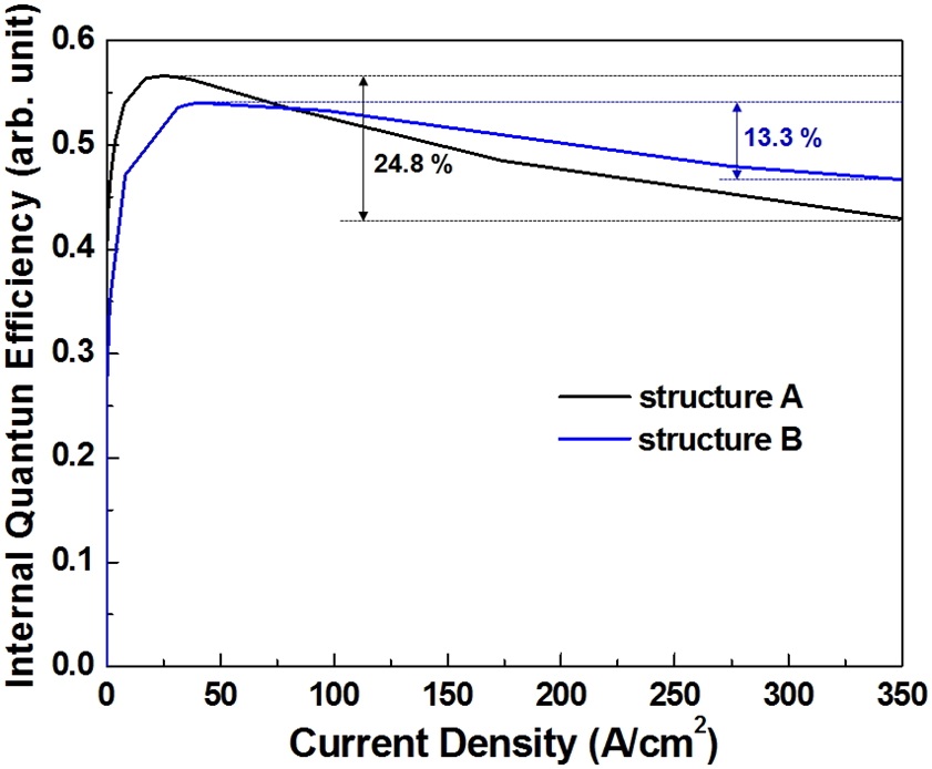
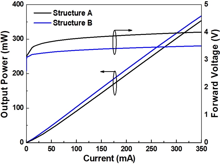
Figure 2 shows the simulated the light-output power versus the current and the current versus the voltage (L-I-V) characteristics for the two LED structures of different quantum barrier types as functions of the injection current. The forward voltages at 350 mA of structure A and B are 4.0 and 3.5 V, respectively. The reduced forward voltage can be attributed to the improvement in the hole injection and distribution by the reduced polarization field of graded-composition AlGaInN barriers. The light output powers of the two LEDs increases as the injection current increases. The output power of structure B was found to be higher than that of structure A over the whole range of current. The light output power of structure B was higher by 4.3% than that of structure A. Also, the IQEs of structure A and B as functions of injection current density are shown in Fig. 3. The IQE of structure B was increased by 9.51% at an injection current of 350 mA compared with that of structure A. The efficiency droop defined as (ηpeak-η350A/cm2)/ηpeak, is alleviated from 24.8% to 13.3%, indicating the improvement of radiative-recombination rate
due to efficient hole injection and distribution. These results indicate that the structure B is the superior one due to the reduced efficiency droop and higher light output power at high current. The cause for the superiority of structure B is the combined effect of the efficient injection and uniform distribution of hole and the enhanced radiative-recombination rates.
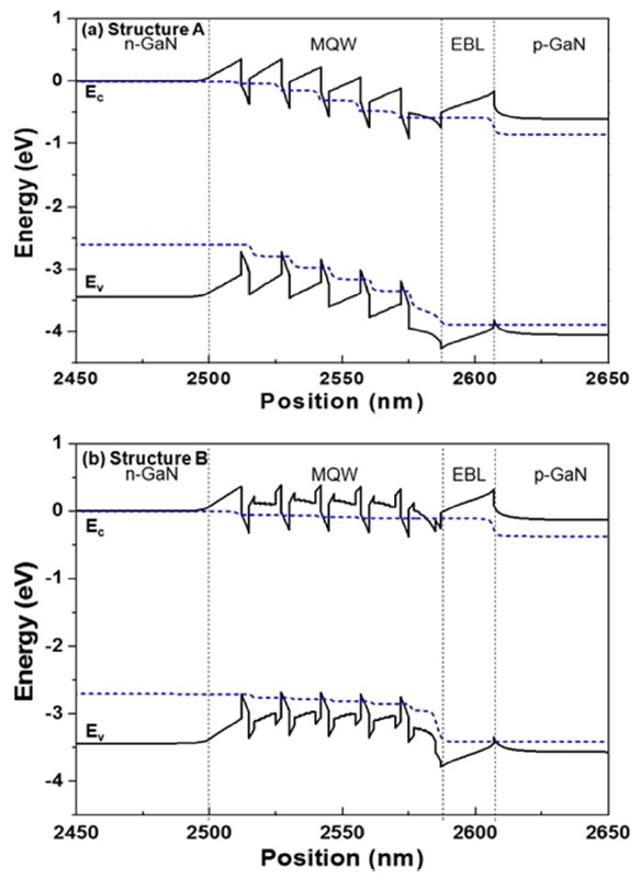
In order to explain the above phenomenon, the calculated energy band diagrams and quasi-Fermi levels of structure A and B at an injection current of 35 A/cm2 are shown in Fig. 4. In Fig. 4(a), the LED with conventional GaN barriers
show highly tilted energy band structures in the active regions. This means that the polarization induced internal field causes the increase of the potential difference in the energy band between the well and barrier layers, and thus the reduction of radiative recombination rate and IQE is occurred by poor overlap between the electron and hole wave functions. In addition, the increased potential height in valence band prevents efficient hole transport from the p-type GaN into active regions. On the other hand, in Fig. 4(b), because of the relative small band bending induced by the
reduced internal field in active regions, the slope of valence band in the inserted graded-composition AlGaInN barriers is alleviated. Therefore, these barriers of structure B can attribute to a decreased effective potential barrier height for the injection and distribution of holes without the leak of electrons out of the active regions.
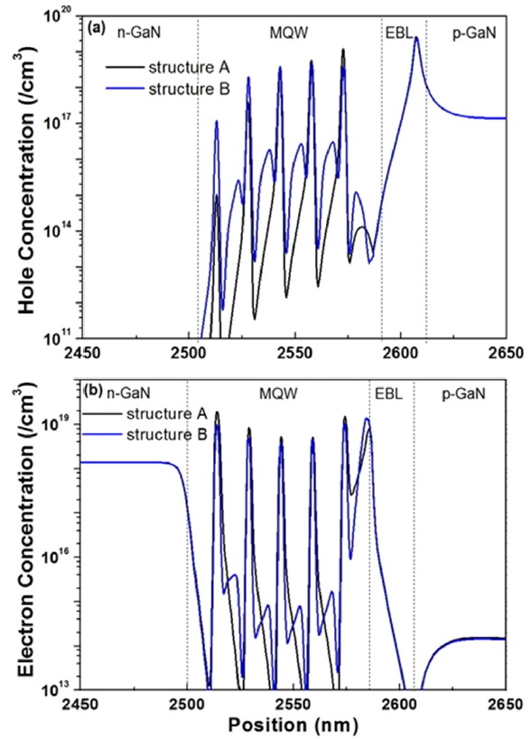
To explain the above-mentioned reasons, the electron and hole concentration of the structure A and B at 35 A/cm2 are shown in Fig. 5. For the structure B, the hole concentration decreased at fifth quantum well near the p-GaN side. However, at the same time, the hole concentrations of first, second and third quantum wells is nearly one or two order of magnitude higher than that of the structure A, which is shown in Fig. 5(a). Simultaneously, electrons are uniformly distributed throughout the entire MQW regions in the structure A and B, as shown in Fig. 5(b). A comparison of the hole concentrations in the structure A and B around the active regions shows a uniform hole distribution for the structure B because the GaN/gradedcomposition AlGaInN/GaN barriers more effectively transport holes. In other words, larger numbers of holes inside the active regions, as well as enhanced overlap of the electron and the hole wave functions, result in the increased radiative recombination. These improved hole injection and distribution results can be further explained by the hole current inside the MQWs.
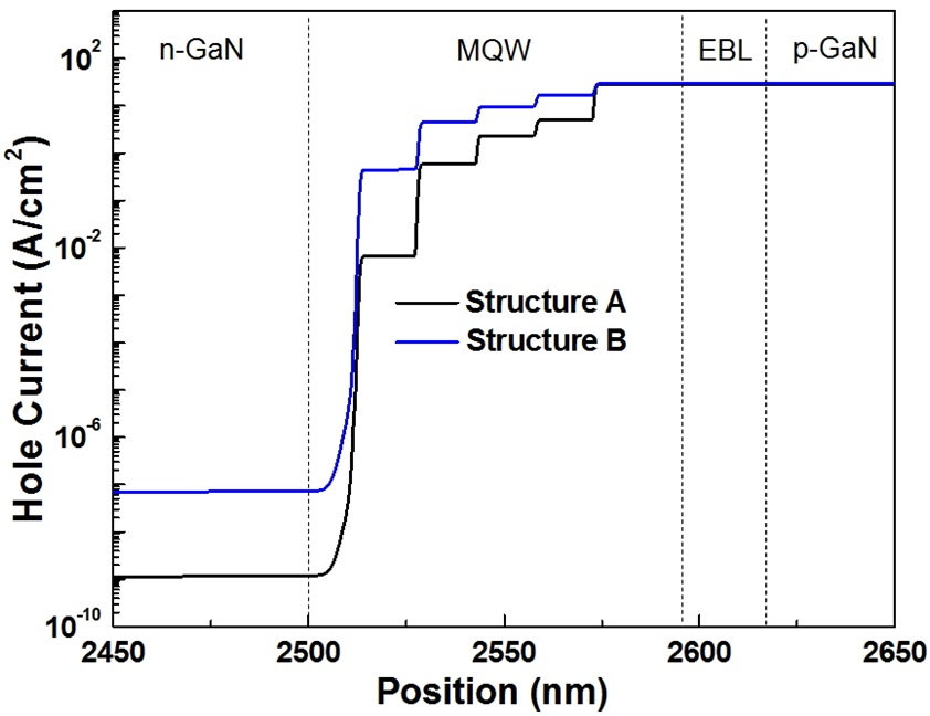
Figure 6 shows the hole injection current densities as functions of position close to the active regions of the LEDs with two different quantum barrier types at 35 A/cm2. The hole current density of the structure B injected into the active region from the p-GaN is higher than that of the structure A. Thus, it is clearly apparent that the GaN/gradedcomposition AlGaInN/GaN barriers enable more efficient hole transport across the MQWs, which is beneficial to the high output power and the reduction of efficiency droop.
In conclusion, we numerically studied the influence of GaN/graded-composition AlGaInN/GaN quantum barriers in the active region on the performance of GaN-based VLEDs. The simulation results showed that, among the two LED structures under study, the LED with GaN/gradedcomposition AlGaInN/GaN quantum barriers revealed the enhanced electrical and optical characteristics. The forward voltages at 350 mA were calculated to be 3.5 and 4.0 V for VLEDs with GaN/graded-composition AlGaInN/GaN barriers and GaN barriers, respectively. The output power and internal quantum efficiency of LEDs with GaN/graded-composition AlGaInN/GaN barriers was higher by 4.3% and 9.51% than those of LEDs with conventional GaN barriers, respectively. The efficiency droop of LEDs using GaN/graded-composition AlGaInN/GaN barriers was alleviated from 24.8% to 13.3%, indicating the improvement of radiative-recombination rate, in comparison with that of LEDs using GaN barriers. Such enhancements could be attributed to the relatively efficient hole injection and uniform distribution in MQWs due to the moderate downward band bending and the high radiative recombination rate in the active regions, and the small efficiency droop. This proposed quantum barrier structure within LEDs is beneficial, especially for GaN-based LEDs operating at high injection current.