In this paper, we propose, analyze and simulate the performances of some new plasmonic logic gates in two dimensional plasmonic waveguides with nanodisk resonators, using the numerical method of finite difference time domain (FDTD). These gates, including XOR, XNOR, NAND, and NOT, can provide the highly integrated optical logic circuits. Also, by cascading and combining these basic logic gates, any logic operation can be realized. These devices can be utilized significantly in optical processing and telecommunication devices.
The prospect of optical processing has motivated extensively recent activities for overcoming the essential performance constraints of semiconductor electronic devices which suffer from inherent delay and high heat generation. Photonic devices which use the photons as information carriers can provide high speed, high capacity and low loss components [1]. The diffraction limit of light has been a fundamental obstacle for reducing the dimensions of optical logic components to the scales of electronic devices in integrated circuits [2,3]. Surface plasmon polaritons (SPPs), the waves created on the surfaces of metals owing to the interaction of the electromagnetic fields in dielectrics and the free electrons in metals, have the most promising applications in the highly integrated optical circuits due to their ability to overcome the diffraction limit of light [4-8].
Therefore, some structures based on SPPs, such as waveguides [9,10], filters [11,12], demultiplexers [13], modulators [14], reflector laser diodes [15], junctions [16], sensors [17,18], and switches [19] have been proposed.
In addition, some all optical logic gates, in nanophotonic plasmonics [20], with hybrid plasmonic-photonic crystal nanobeam cavities [21], and based on waveguide type Kretchman-Reather configuration on the metal surface [22] have been proposed and analyzed. Also, some other logic gates based on silicon micro-ring resonators [23], two photon absorption in silicon waveguides [24], cross phase modulation [25], and single semiconductor optical amplifiers have been investigated [26].
Some of these devices employ the effects of electro-optic or magneto-optic by applying respectively an electric or magnetic field, which has some disadvantages in switching time, loss and size [27,28].
Recently, some plasmonic structures based on the nanodisk resonators such as filters and demultiplexers have been investigated [11,13,29-31]. In this paper, some basic plasmonic logic gates of XOR, XNOR, NAND, and NOT, in simple plasmonic structures with nanodisk resonators are proposed and investigated numerically and analytically. The simulation results obtained by the FDTD method can verify the effects of variations of the structural parameters on the performances of the gates.
Design and implementation of more complex logic gates can be accomplished by combining and cascading these logic gates appropriately. Their performances can be adjusted by variation of the structural parameters to achieve desired operations.
Plasmonic logic gates can highly reduce the sizes and hence the signal losses, decrease the signal thresholds for the logic operations, and can provide fast switching optical devices. Our proposed structures can operate in a wide range of frequency and create developments in nano optic processors for optical computing technologies. The proposed structures are a few hundreds of nanometers in size. The structures are simple and by utilizing the current advanced nanolithography techniques, with which is possible to design and implement devices with accuracy of 5 nm in size, can be realized for photonic integrated circuits (PICs) [32].
The paper is organized as follows: In Section II, the main structure is proposed and its performance is analytically investigated. In Section III, the simulation results of the proposed plasmonic logic gates are presented and verified analytically. In Section IV the effects of variation of the structural parameters are demonstrated, and finally the paper is concluded in Section V.
II. THE STRUCTURE AND THE METHOD OF THEORETICAL ANALYSIS
Our proposed structure is based on the simple nanodisk resonator, shown in Fig. 1. The input and output waveguides are coupled in the resonance frequencies of the nanodisk.
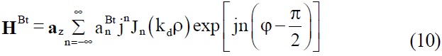
Let us assume that a TMx plane wave is incident upon a two dimensional circular disk. The incident, scattered and transmitted fields, by imposing the boundary conditions for tangential electric and magnetic fields at the surrounding surface of the disk, can be expressed as [33]:


where the subscripts i, s, and t correspond to the incident, scattered and transmitted fields. The coefficients an i, an s, and
an t are the amplitudes of the incident, scattered and transmitted fields, respectively. ηd and ηm represent the intrinsic impedances of dielectric and metal, respectively.
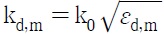
are the wave numbers in the dielectric and metal, k0 is the free space wave number and εd and εm are the permittivity of dielectric and metal, respectively. a is the radius of the disk. Jn, Hn (l), Jn ', and Hn (l)' signify the first kind Bessel function, the first kind Hankel function of the order n and their derivatives, respectively. The metals have been assumed to be silver whose relative permittivity function can be described by the Drude model. For the time variation of exp(-jωt), the model can be expressed as [34]:
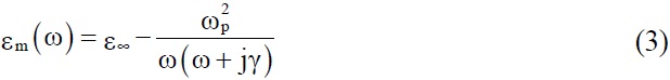
where ε∞ is the dielectric permittivity at the infinite frequency and ω is the angular frequency of the incident lightwave. The material-dependent constants ωp and γ are the bulk plasma and damping angular frequencies, respectively. The Drude parameters for silver can be assumed as ε∞ = 3.7, γ = 0.018eV, and ωp = 9.1eV [29].
We can solve Eqs. (1) and (2) for unknown coefficients an t and an s. For a nontrivial solution, the determinant of the matrix of the coefficients must be zero to attain:
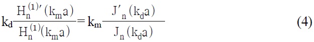
The resonance frequencies of a disk with radius a and specified electrical parameters can be obtained by solution of Eq. (4).
III. SIMULATION RESULTS AND DISCUSSIONS
3.1. General Aspects of Simulation
In this paper, a two-dimensional FDTD scheme is applied to analyze the properties of the structure with the convolutional perfectly matched layers (CPML) absorbing boundary conditions at all boundaries of the simulation domain [34]. The grid sizes in the x and y directions are Δx = Δy = 5 nm and the time step, derived by the Courant condition is
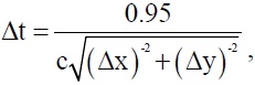
where c denotes the speed of light in free space [34]. The incident lightwave for excitation of the SPP mode is a TMx-polarized plane wave (the magnetic field is parallel to z axis). The structural parameters are set as a = 200 nm, d = 10 nm, w = 50 nm, and the dielectric material is considered air with refractive index of 1.
In addition, we can calculate the ON/OFF ratio of the proposed gates as a figure of merit of the structures. The ON/OFF ratio can be defined as:
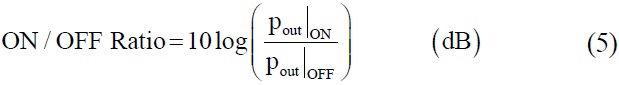
where pout|ON and pout|OFF are the output power at high and low logic states, respectively. We have considered the levels of normalized transmission of 1.9-4.2 as the high logic state, and normalized transmission of 0.001-0.002 as the low logic state.
Now we introduce the proposed logic gates.
The Exclusive-OR (or simply XOR) operation is defined functionally as [35]:

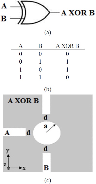
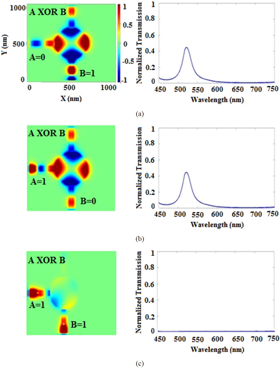
The standard logic symbol, the truth table, and the structure of the proposed XOR logic gate, are presented in Fig. 2. The output of the XOR gate is 1 (high) if and only if its inputs are not simultaneously equal. In other words, when the inputs are different, the output is 1. We can verify these relations in our proposed XOR structure. The inputs of the gates are two sources of A and B as shown in Fig. 2(c). The simulation results of the proposed XOR gate are demonstrated in Fig. 3. The performance of the gate can be verified by the following analytic discussion.
We suppose that the incident electromagnetic fields of the sources A and B propagate in the x and y directions, respectively. We can consider the magnetic fields of the two different inputs as follows:

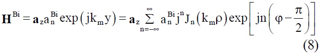
where an Ai and an Bi are the intensities of the two sources. ρ and φ denote radial distance, and azimuth angle, respectively. The corresponding transmitted magnetic fields to the nanodisk will be:

Since:

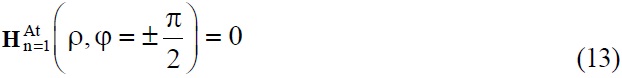
using Eqs. (9) and (10) for n = 2, and when anAi = anBi ≠0 (both of the inputs are in high logic state), the total magnetic field, can be found as:

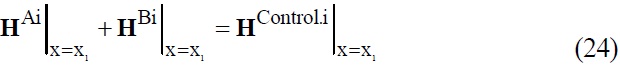
and consequently the second resonance mode cannot be transmitted to the output and provides the low logic state. Therefore, we use the second resonance mode of the nanocavity to realize our proposed logic gate. Here, the two inputs A and B are assumed to be simultaneously equal. Obviously, if they are not equal, Eq. (12) does not hold and therefore, the output will be in high logic state. Eqs. (9)-(12) imply that for proper operation, the intensities of the sources of the proposed gate must be exactly equal. Furthermore, the location of the two input sources must be in the same distance to the nanodisk, to avoid the differences in intensities at the nanodisk caused by the loss along propagation. In the proposed structure, two factors are used to provide the pi phase difference, when both of the inputs A and B are in high logic state: 1. 90 degrees angle between the input waveguides, 2. The resonating of the second resonance mode which creates pi phase difference, the results of which will be wave cancellation.
We can describe the structure qualitative performance, as follows. When for example, two inputs A and B are in high
logic state, the feeder sources (A and B) excite plasmonic waves along the waveguides. Two travelling modes propagating in two waveguides are coupled into the nanodisk and create steady-state mode-field patterns at resonance wavelength of the nanodisk. Fig. 3 exhibits the mode-field distribution of magnetic field. Because of the symmetry of the sources, and due to the out of phase waves from two sources of A and B, the waves diminish each other and provide a null mode in the output waveguide to provide low logic state (Fig. 3(c)).
According to Eq. (5) and based on the simulation results of Fig. 3, the ON/OFF ratio is 26 dB at the wavelength of 525 nm (according to the second resonance mode of the nanodisk).
Although in Fig. 3, we have shown the gate performance using a continuous wave source at specific wavelength corresponding to the second resonance mode of the nanodisk to illustrate its proper performance, but we can apply a pulse source in the general case (square pulse, Gaussian pulse, etc.) as it is common in digital systems and includes a wide spectrum of frequency. In fact the proposed structure can play as a band-pass filter at the resonance wavelengths of the nanodisk [29]. Therefore, if we apply pulse sources, only the wavelengths corresponding to the resonance wavelengths can transmit to the outputs of the gates. Among these transmitted wavelengths, the second resonance mode is the preferable mode. The higher resonance modes have negligible effect and can be ignored. The most critical problem is the first resonance mode. It can disturb the performance of the gate. It can easily change an ON state to an OFF one, and vice versa because this mode cannot be transmitted from the 90 degree branch to the output. We can verify this behavior by considering Eqs. (9)-(11), for n = 1. The magnetic field due to the source A in output, can be found as:
and consequently the first resonance mode due to the source of A, cannot be transmitted to the output and only one source is involved during the transmission of the first mode (source B according to Fig. 3). Consequently, if we prevent the transmission of the first mode, we can overcome this problem.
As a result, we can apply any kind of pulse such as square, modulated Gaussian, etc. to drive the proposed gate to achieve the ON logical state, properly. In simulation, a Gaussian modulated pulse has been applied.
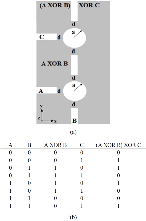
We can use two proposed XOR gates as two serially connected components as shown in Fig. 4(a). The structure performance can be deduced from the truth table of Fig. 4(b). The second gate can also act as another XOR gate, like the first one. Both of them operate in the second resonance mode as we can derive from Eqs. (7-10). However, the output of the first gate (the input of the second gate) suffers from SPP losses. So, this wave must be amplified using the active plasmon or gain media, to increase the intensity to the level of the input C in Fig. 4(a) to guarantee the proper performance of the second gate.
A common function that is related to the exclusive-OR is the coincidence operation, or exclusive-NOR (XNOR), which is merely the complement of the exclusive-OR. This function is defined as follows:

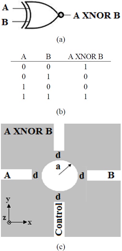
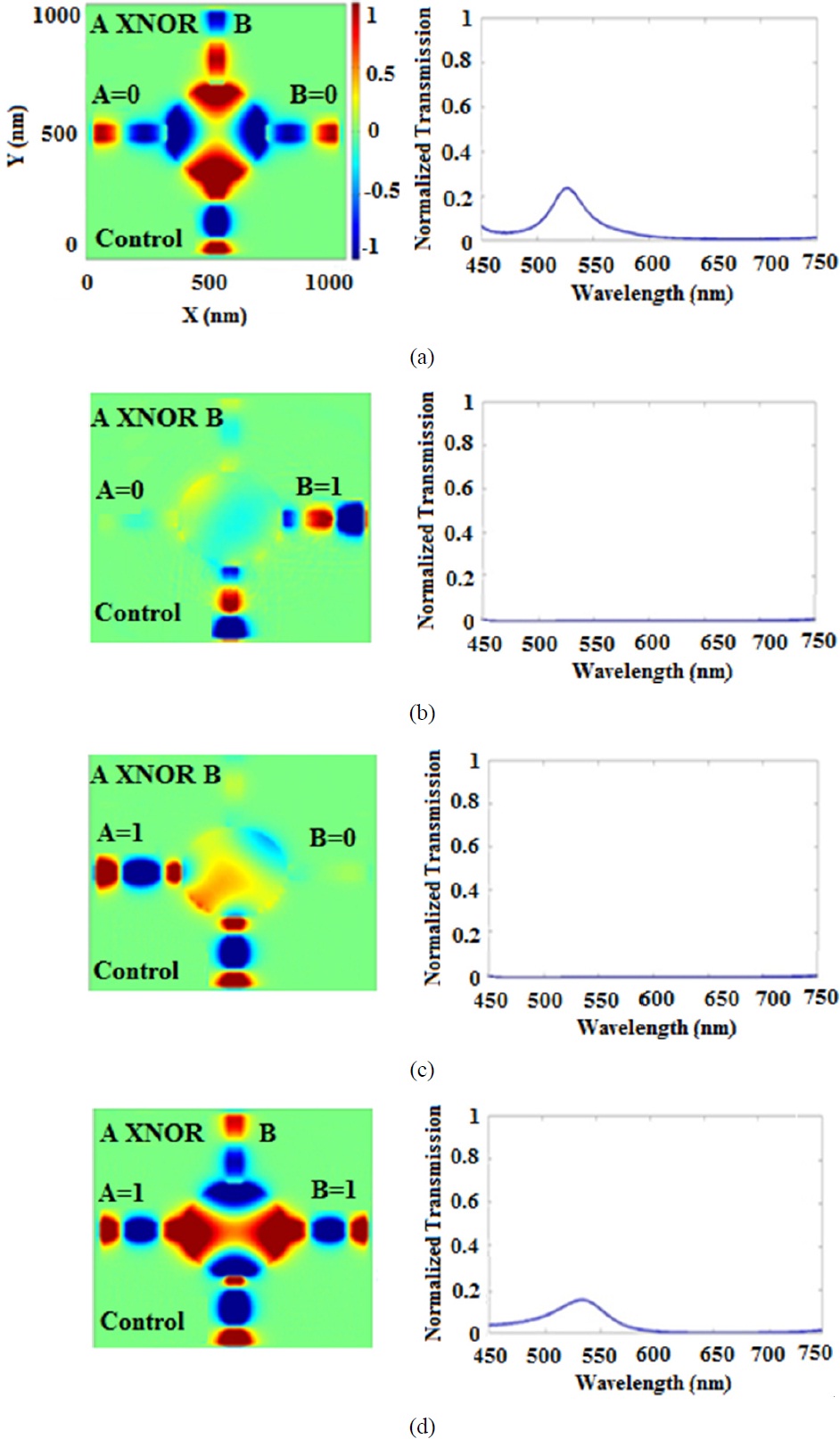
The XNOR gate symbol, the truth table, and the proposed structure are presented in Fig. 5, and the simulation results of which are illustrated in Fig. 6.
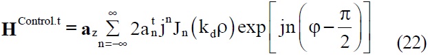
Our proposed gate requires one control port to perform the XNOR functionality, which may be considered as a drawback. This control port must always be in the ON state.
The analytic verifications are similar to the XOR gate. We suppose that the incident electromagnetic fields of the similar sources of A, B, and control, whose intensities are equal, propagate in the x, -x, and y directions, respectively. Therefore, the corresponding transmitted magnetic fields to the nanodisk will be:


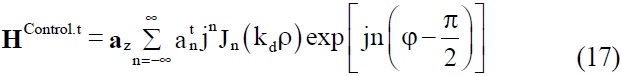
Therefore, using Eq. (11), for the second resonance mode (n = 2), the total magnetic field can be found as:

and consequently the second resonance mode can be transmitted to the output. Therefore, if two inputs A and B are simultaneously in high logic state, the output will be in high state. When one of the inputs A or B are in low state, two other waves diminish each other, and consequently, no wave will be transmitted to the output and the output will be turned into the low logic state. According to the simulation results, there are two values for peak transmission as high logic values (corresponding to Figs. 6(a) and 6(d)). Therefore, the ON/OFF ratio can be calculated to be equal to 24 and 23 dB at wavelength of 525 nm, accordingly.
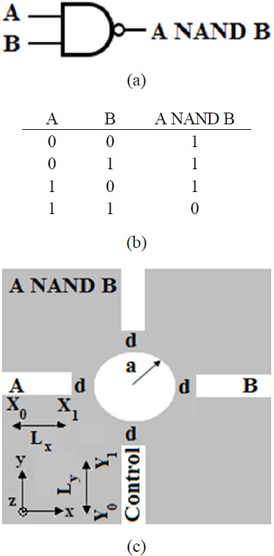
In fact a NAND gate is a combination of an AND gate followed by a NOT gate. The NAND function is defined as:

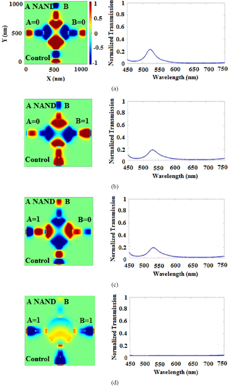
The output is 0 if and only if its inputs are simultaneously 1 and is 1 for other cases. The standard NAND gate symbol, the truth table, and the basic structure are shown in Fig. 7. The simulation results are illustrated in Fig. 8. Again one control port is required, which must always be in ON state (Fig. 7(c)). The field intensity of the control wave must be twice the input intensities to diminish summation of the input waves and provide low logic state at the output when A = B = 1. By utilizing the control port, there are two different procedures to achieve this performance, the analyses of which are discussed as follows:
a) A source with field intensity twice the input intensities at the control port is used. The transmitted magnetic fields in the nanodisk due to three sources A, B, and control will be:


For the second resonance mode (n = 2) we can find:

and consequently the second resonance mode cannot be transmitted to the output and provide the low logic state. If either or both of the sources of A and B be in the low state, Eq. (23) does not hold and the output will be in high state.
b) The relative location of the input and control sources can be adjusted to provide the desired intensity at the nanodisk.
The three similar sources are supposed to be at different locations in the proposed NAND structure (Fig. 7(c)). To realize low logic state, two input waves must be diminished by the wave from the control source:
If we consider the input sources; intensities equal:
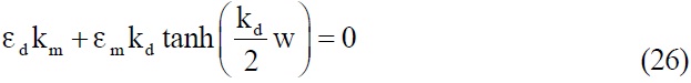
It can be assumed that the transmitted waves propagate as plane waves along the waveguides. Since the widths of the waveguides are much smaller than the incident wavelength, only one propagation mode (TM0) can exist in the waveguides, the propagation constant of which (β= βR + jβI) can be obtained by solving the following dispersion equation [36]:
where:

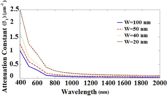
Figure 9 shows the calculated attenuation constant (imaginary part of β, βI) spectra for different widths of the waveguides.
Using Eq. (25), for propagation length of Lx and Ly in x and y direction, respectively, we can find:
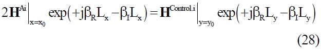
By considering the absolute value of Eq. (28) and assuming similar sources at input and control ports:

According to Fig. 9, we find that for a waveguide with width of 50 nm, the value of βI equals 0.5 μm-1. Using Eq. (29), |Lx - Ly| is equal to 1400 nm. Referring to Fig. 9, for shorter widths, βI is higher. Hence, the difference in location (|Lx - Ly|) is lower. However, this approach has some disadvantages in size of the structure. So, we prefer to choose the first procedure.
Due to the simulation results, there are two values for peak transmission as high logic values (corresponding to Figs. 8(a)-(c)). Hence, we can calculate the ON/OFF ratio to be equal to 23 and 21 dB in wavelength of 525 nm, accordingly.
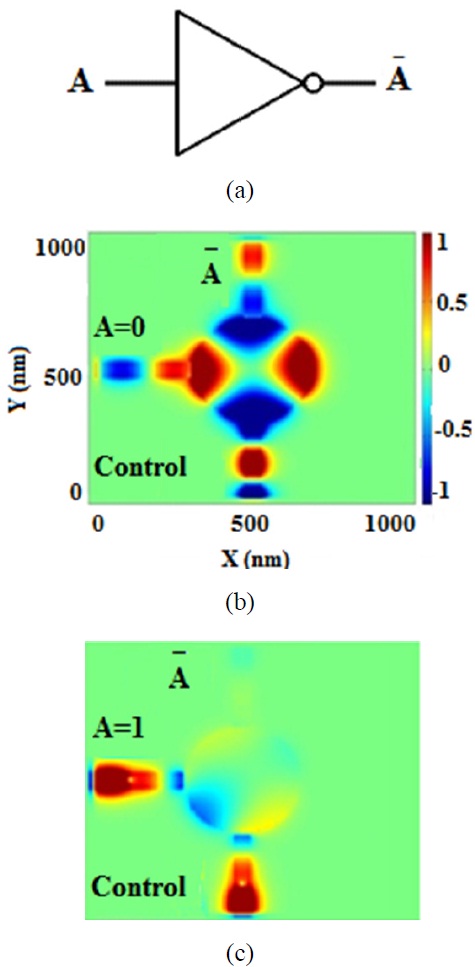
A NOT gate, or inverter, is used to implement the complement concept in switching algebra. The standard symbol for a NOT gate is shown in Fig. 10(a). The logic value of the output of a NOT gate is simply the complement of the logic value of its input:

In fact our proposed NOT gate is a XOR gate with a control port. The control port must always be in the ON state. For example if we set the input B, 1, as the control port, the output can be considered the complement of the other input (A). The analytic verification is similar to that of the XOR gate, when one of the inputs is considered as the control port.
IV. THE EFFECT OF VARIATIONS OF STRUCTURAL PARAMETERS
Variations of the structural parameters have multiple effects
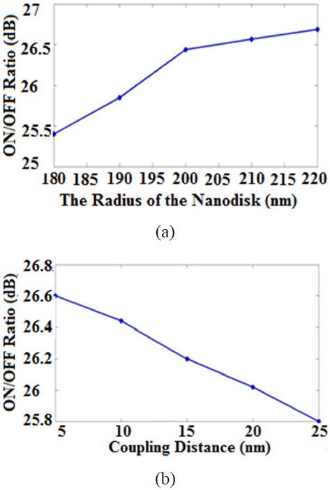
on the behavior and performance of the proposed structures. The resonance wavelength of transmission and the bandwidth of the resonance spectra can be adjusted by these variations appropriately [29]. Now we want to study the effects of the variations of the structural parameters on the ON/OFF ratio, as a figure of merit of the structure. We have investigated these changes for one of the proposed structures, say the XOR gate.
4.1. Variations of the Nanodisk Radius
When the radius of the nanodisk increases, the transmission for the second resonance wavelength will increase [29]. Therefore, pout|ON will increase, while pout|OFF will have negligible change. So, the ON/OFF ratio will be improved as shown in Fig. 11(a).
4.2. Variations of the Coupling Distance
When the coupling distance of the nanodisk and waveguides increases, the transmission will decrease [29]. Therefore, pout|ON will decrease, while pout|OFF will have negligible change. So, the ON/OFF ratio will be deteriorated as depicted in Fig. 11(b).
In this paper, some plasmonic logic gates such as XOR, XNOR, NAND, and NOT gates have been proposed and investigated using the numerical method of FDTD. These simple and compact devices can be utilized in photonic integrated circuits (PICs). Their behaviors and performances can be adjusted by variation of the structural parameters. Our proposed XOR gate seems to be more advantageous, since it does not require any control ports, which can be regarded as a disadvantage. The proposed gates behaviors have been verified analytically. The simulation results have been in good agreement with those of the analytic ones.