Bounding the worst-case DRAM performance for a real-time application is a challenging problem that is critical for computing worst-case execution time (WCET), especially for multicore processors, where the DRAM memory is usually shared by all of the cores. Typically, DRAM commands from consecutive DRAM accesses can be pipelined on DRAM devices according to the spatial locality of the data fetched by them. By considering the effect of DRAM command pipelining, we propose a basic approach to bounding the worst-case DRAM performance. An enhanced approach is proposed to reduce the overestimation from the invalid DRAM access sequences by checking the timing order of the co-running applications on a dual-core processor. Compared with the conservative approach, which assumes that no DRAM command pipelining exists, our experimental results show that the basic approach can bound the WCET more tightly, by 15.73% on average. The experimental results also indicate that the enhanced approach can further improve the tightness of WCET by 4.23% on average as compared to the basic approach.
With the rapid development of computing technology and the diminishing return of complex uniprocessors, multicore processors are being used more widely in the computer industry. Future high-performance real-time systems are likely to benefit from multicore processors due to the significant boost in processing capability, low power consumption, and high density.
In real-time systems, especially hard real-time systems, it is crucial to accurately obtain the worst-case execution time (WCET) for real-time tasks to ensure the correctness of schedulability analysis. Although the WCET of a real-time application can be obtained by measurement- based approaches, the results are generally unreliable due to the impossibility of exhausting all the possible program paths. Alternatively, static WCET analysis [1] can be used to compute the WCET, which should be safe and as accurate as possible. The WCET of a real-time application is not only determined by its own attributes, but also affected by the timing of architectural components, such as pipelines, caches, and branch predictors. Most prior research works have focused on WCET analysis for single-threaded applications running on uniprocessors [2-6], but these methods cannot be easily applied to estimate the WCET on multicore processors with shared resources, such as a shared L2 cache and DRAM memory. This is because the possible interferences in the shared resources between different threads can significantly increase the complexity of WCET analysis.
Due to its structural simplicity, high density, and volatility, DRAM is usually utilized in current popular processors, including multicore processors. A DRAM system consists of multiple components, such as a memory access controller, command/address bus, data bus, and DRAM devices. The latency of an access to the DRAM varies due to the status of each component when accessed. One recent work studied the vulnerability of current multicore processors due to a new class of denial of service (DoS) attacks [7]. Under the current DRAM architecture, a thread with a particular memory access pattern can overwhelming the shared resources in the DRAM, preventing other threads from using these resources efficiently. Therefore, the latencies of the DRAM accesses from other threads could be prolonged.
There have been several studies to model and predict DRAM memory performance. Ahn et al. [8] performed a performance analysis of scientific and multimedia applications on DRAM memory with various parameters, and found that the most critical performance factors are high read-write turnaround penalties and internal DRAM bank conflicts. They then developed an accurate analytical model for the effective random-access bandwidth given DRAM technology parameters and the burst-length. Yuan and Aamodt [9] proposed a hybrid analytical model to predict DRAM access efficiency based on memory trace profiling. Bucher and Calahan [10] modeled the performance of an interleaved common memory of a multiprocessor using queuing and simulation methods. Choi et al. [11] presented an analytical model to predict the DRAM performance based on the DRAM timing and memory access pattern parameters. However, these prior studies have focused on predicting the average-case DRAM performance, rather than the worst-case. For example, the DRAM access patterns assumed in these studies were based on typical access patterns or derived from simulated traces, which cannot be safely used to represent the worst-case DRAM access patterns to derive the WCET.
Research was performed recently to bound the worstcase DRAM performance on a uniprocessor by considering the impact of the row-buffer management policy [12]. However it is more challenging to conduct WCET analysis on a multicore processor by bounding the worst-case DRAM performance for the following reasons. First, the DRAM access pattern of a thread depends on its accesses to higher-level cache memories, such as the L2 cache. If the DRAM memory is shared with different cores, the accesses of a thread can be greatly impacted by inter-core DRAM access interference. Second, the worse-case latency of a DRAM access of a thread is determined by not only the number of the simultaneous DRAM accesses from other threads, but also the timing order of all these DRAM accesses and the spatial locality of the data fetched by them. However, the timing order of simultaneous DRAM accesses from co-running threads is hard to determine through static analysis, because all the threads are running independently on different cores.
To overcome these difficulties, this paper first investigates the timing characteristics of DRAM accesses with a focus on DRAM devices. Our study shows that the DRAM commands from multiple consecutive DRAM accesses can be pipelined on DRAM devices, and the degree of the DRAM command pipelining varies according to the spatial locality of the data accessed, which may impact the worst-case latency of each access. A basic approach is then proposed to estimate the worst-case situation of DRAM command pipelining, which leads to the worstcase latency for a DRAM access among a sequence of consecutive DRAM accesses. An enhanced approach is proposed to reduce the overestimation from the invalid DRAM access sequences by checking the timing order constraints of concurrent applications. In addition, we utilize the extended integer linear programming (ILP) approach [4] to model the constraints between the accesses to the higher-level cache memory and the DRAM accesses. The worst-case DRAM performance is integrated into the objective function of the extended ILP approach to bound the WCET of a real-time task running on a multicore processor.
The rest of the paper is organized as the follows. First, the multicore architecture studied in this work is described in Section II. Next, the background of the DRAM system is introduced in Section III. Section IV presents the timing characteristics of DRAM accesses, with a focus on DRAM devices. Then, we introduce two approaches to bound the worst-case DRAM performance in Section V. Section VI introduces the evaluation methodology, and Section VII gives the experimental results. Finally, conclusions are presented in Section VIII.
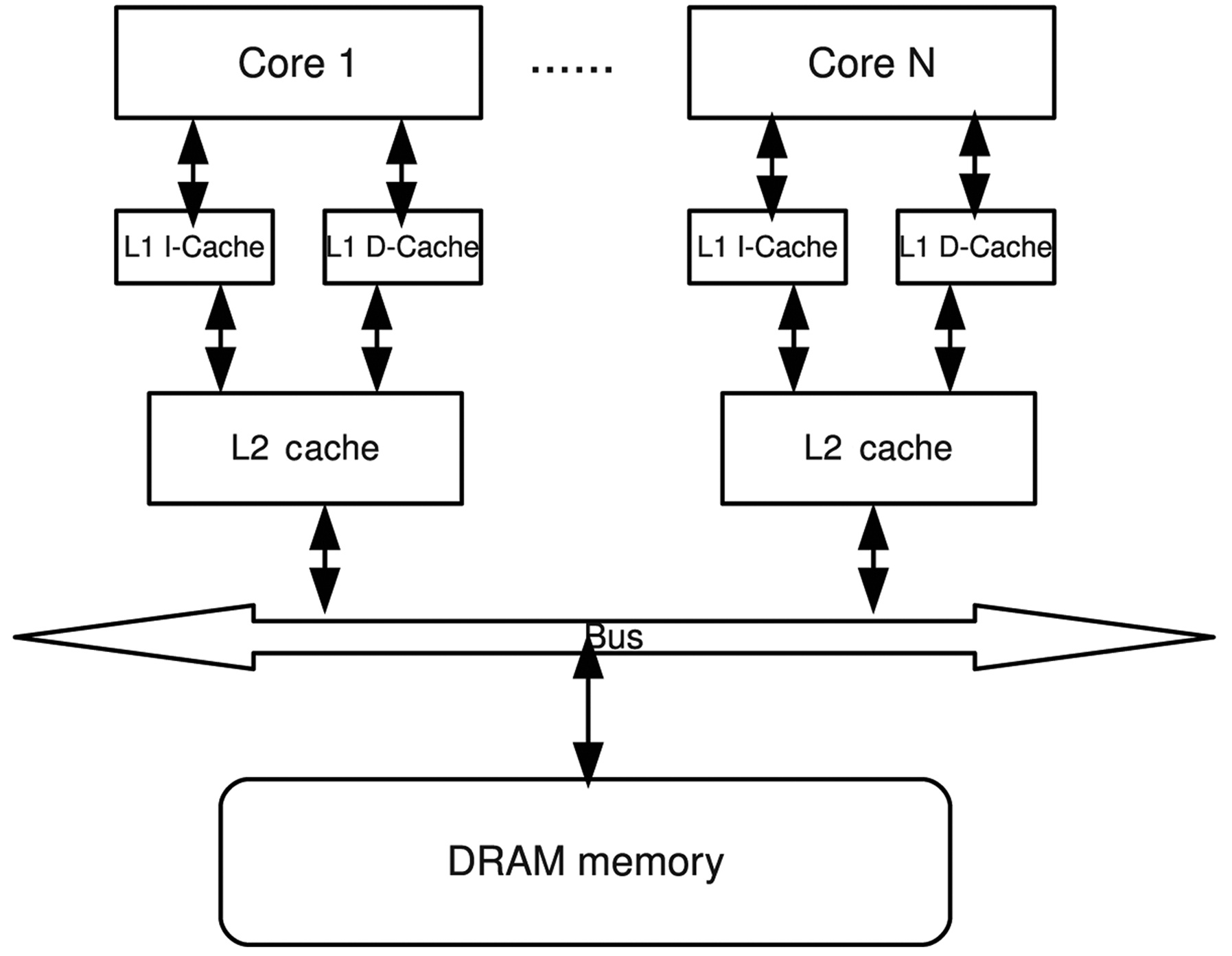
Fig. 1 shows the system architecture of a multicore processor with
core is symmetrical, with its own processing unit, pipeline, L1 instruction and data caches, and private L2 cache, which are not uncommon in commercial multicore designs. The DRAM is shared by all cores through a shared bus. In order to focus on bounding the worst-case DRAM performance, the interactions between the DRAM and the hard disk are ignored in our study. It is assumed that all the code and data of a thread are loaded into the DRAM beforehand, such that no page fault would occur during subsequent execution.
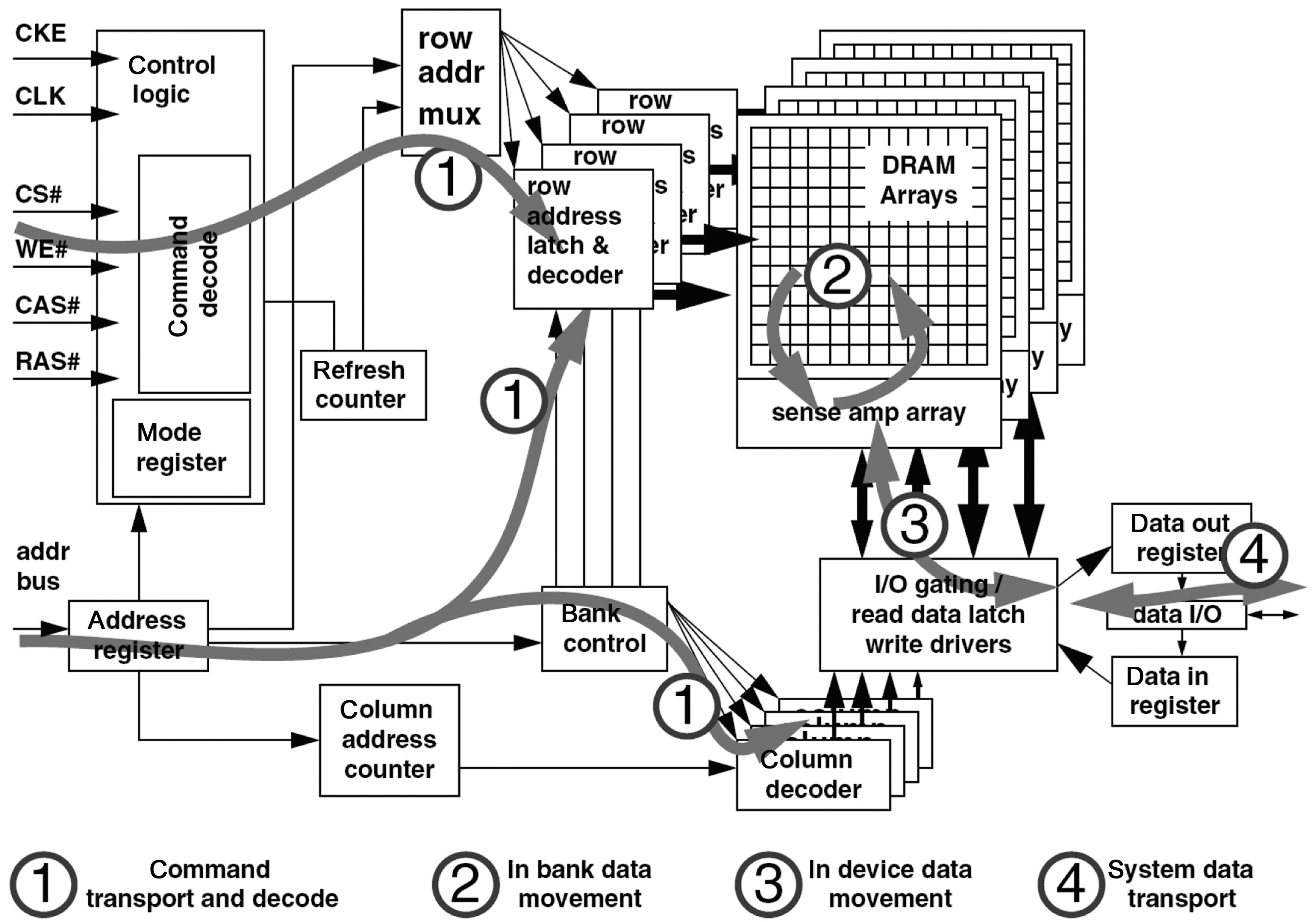
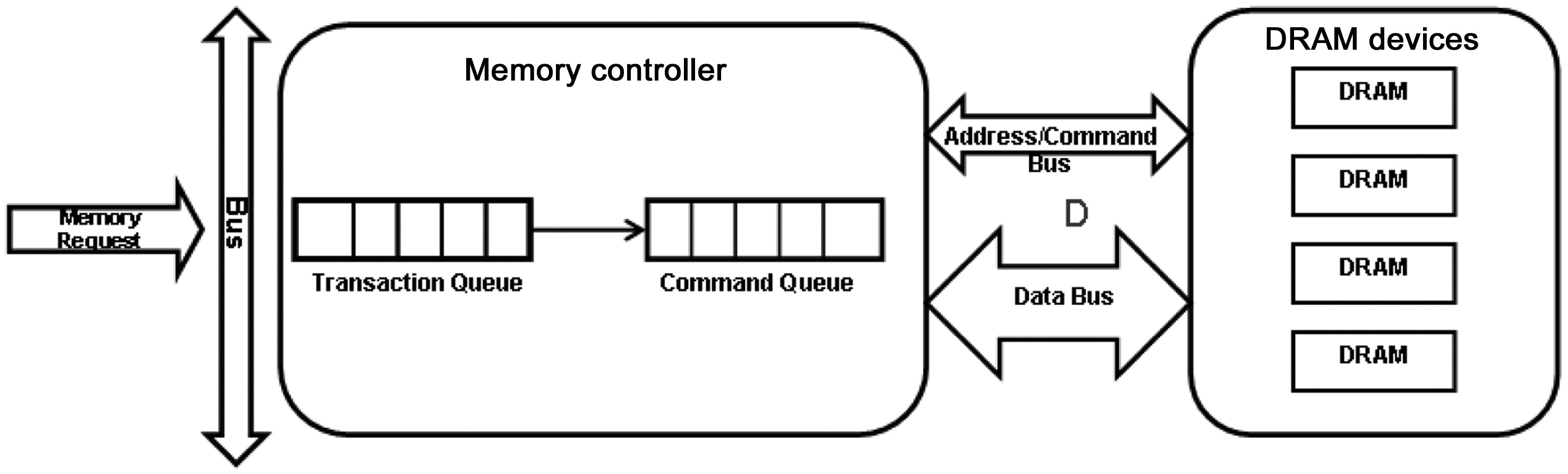
Generally, a DRAM memory system comprises three major components, as shown in Fig. 2. The DRAM devices store the actual data; the memory controller is responsible for the communication between the DRAM devices and the processor; and the buses connect the DRAM devices and the memory controller to transfer addresses, commands, and data.
DRAM device: Multiple levels of store entities are organized hierarchically in a DRAM device, such that DRAM accesses can be served in parallel on a certain level according to the spatial locality of the data being accessed. The memory array is the fundamental storage entity in a DRAM device. A bank is a set of independent memory arrays, and has a two-dimensional structure with multiple rows and columns. A bank also has a row buffer, and data can only be read from this buffer. A rank consists of a set of banks sharing the same I/O gating, and operates in lockstep to a given DRAM command. A channel is defined as a set of ranks that share the data bus. For example, multiple DRAM accesses to different ranks in the same channel can be executed in parallel, except when the data are transferred on the shared data bus.
Memory controller: The memory controller manages the flow of data in and out of DRAM devices connected to it. The row-buffer management policy, the addressing mapping scheme, and the memory transaction and DRAM command ordering scheme are three important design
considerations and implementations for the memory controller.
There are two types of row-buffer management policies: the open-page policy and the close-page policy. The open-page policy is designed to favor memory accesses to the same row of memory by keeping the row buffer open and holding a row of data for ready access. In contrast, the close-page policy is designed to favor accesses to random locations in the DRAM, and optimally supports the DRAM access patterns with low degrees of spatial locality. In a multicore processor, the intermixing of DRAM access sequences from multiple threads reduces the spatial locality of the access sequence. The closepage policy can achieve better performance [13] without any optimization on the memory controller [14]. The DRAM access transactions and DRAM commands are queued in the memory controller. The queuing delay also affects the performance of DRAM. DRAM commands can be scheduled by various scheduling algorithms [15,16] based on different factors, such as the availability of resources in DRAM devices. In our study, the memory controller is assumed to have no optimization, and the close-page policy and the first come first serve (FCFS) scheduling algorithm are used.
IV. TIMING OF ACCESSING DRAM MEMORY SYSTEMS
In this section, we study the timing characteristics of the DRAM access, both in the case of an individual DRAM access and multiple consecutive DRAM accesses. Also, the worst-case latency for a DRAM access among a sequence of consecutive DRAM accesses is derived.
Generally, the timing of a DRAM access consists of three parts: the latency through the bus between the processor and the memory controller, the queuing delay in the memory controller, and the latency of accessing the DRAM device. In this paper, as we focus on the estimation of the latency of accessing DRAM devices, the worst-case bus latency and the worst-case queuing delay in the memory controller are estimated safely as constants by a conservative approach, assuming that a given DRAM access from one core should wait for the bus transferring and the memory controller queuing of the other
>
A. Generic DRAM Access Protocol
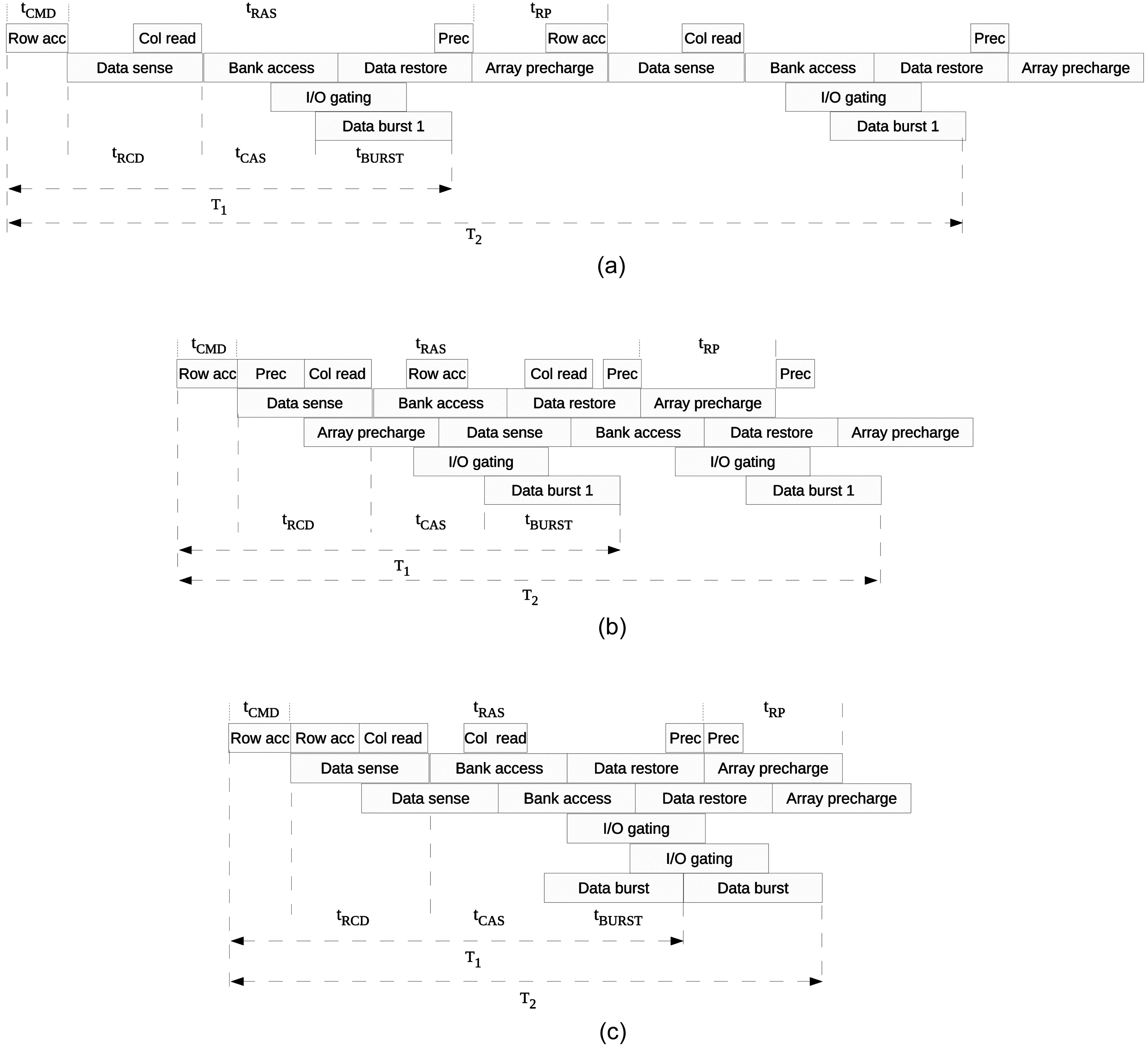
Typically, a DRAM access can be translated into several DRAM commands to move data between the memory controller and the DRAM devices. A generic DRAM access protocol can be modeled by only considering some necessary basic DRAM commands and related timing constraints. It is assumed that two different commands can be fully pipelined on a DRAM device only if they do not have any conflict on a shared resource at a given time, which can be called DRAM command pipelining. The whole procedure for DRAM commands of a given DRAM access to fulfill the data movement are illustrated in Fig. 3. The figure also shows the resources required by these commands that cannot be shared by the commands from other DRAM accesses concurrently. In the first phase, the command is transported via the command and address buses and decoded by the DRAM device. In the second phase, the data are moved into a bank. The data are transported on the shared I/O gating circuit in the third phase. Finally, the data are transferred to the memory controller by the data bus.
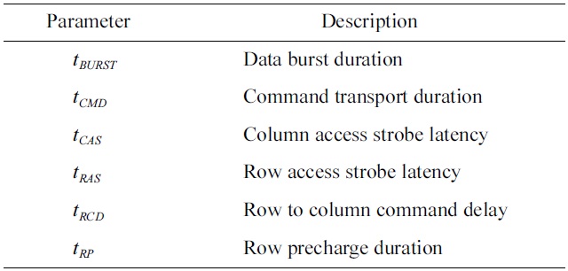
In the generic DRAM access protocol, three generic DRAM commands are defined: row access commands, column access commands, and precharge commands. The timing parameters related to these commands are shown in Table 1.
[Table 1.] Timing parameters defined in the generic DRAM access protocol

Timing parameters defined in the generic DRAM access protocol
in Fig. 4. The DRAM refresh command is not covered in the generic DRAM protocol, because it is not issued from any DRAM access, and could interrupt the command pipeline periodically.
>
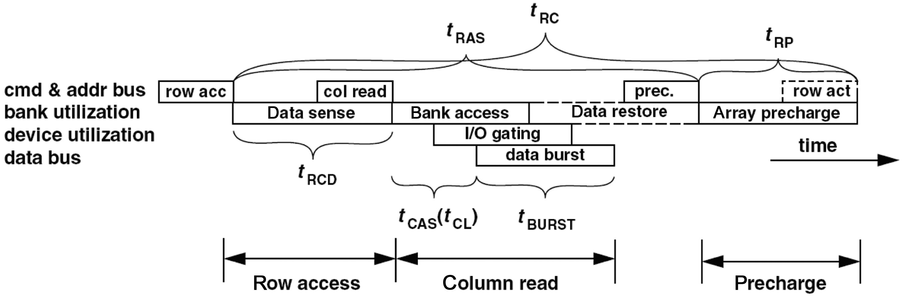
B. Timing of an Individual DRAM Device Access
A typical cycle of an individual DRAM device access to read data consists of three major phases: row access, column access, and precharge. The details of the cycle are illustrated in Fig. 4. Including the time of command transferring, the latency for the whole cycle can usually be computed by using Equation (1), the timing parameters of which are illustrated in Fig. 4. As the data movement for a DRAM access is finished at the end of the column access, the latency of a read cycle without considering the precharge phase can be described by Equation (2), the timing parameters of which are also shown in Fig. 4.


>
C. Timing of Consecutive DRAM Device Accesses
Multiple consecutive DRAM accesses happen more frequently on a multicore processor than on a uniprocessor for the following reasons. First, the number of DRAM accesses issued concurrently increases as the number of cores increases. Second, there is no data dependency or control flow constraint between the DRAM accesses from the threads running on different cores. However, the DRAM commands of consecutive DRAM accesses can rarely be fully pipelined, because these commands need to share resources in the DRAM devices concurrently. The degree of the DRAM command pipelining depends on the spatial locality of the data fetched by the consecutive DRAM accesses, as well as the state of the DRAM devices, which can possibly impact the latency of a DRAM access among a sequence of consecutive DRAM accesses.
Fig. 5 demonstrates the latencies of two consecutive DRAM device accesses in three cases with different data spatial locality between them. Both DRAM accesses are ready to be executed at the same time. The latency of the first access


It can easily be concluded that the later of two consecutive DRAM accesses will have the worst-case latency if both accesses fetch data on the same bank. Furthermore, it can be extended to the case of

V. ANALYZING WORST-CASE DRAM PERFORMANCE
Our assumptions: In this work, we develop a WCET analysis method to derive the WCET for real-time applications running on multicore processors by modeling and bounding the worst-case DRAM performance. We focus on studying the instruction accesses through the memory hierarchy, and assume the data cache is perfect. Also, in our WCET analysis, we have not considered the timing
caused by bus conflicts and DRAM memory refreshing. We assume in-order pipelines without using branch prediction. In our software model, we assume a set of independent tasks execute concurrently on different cores, and there is no data sharing or synchronization among those tasks.
We extend the implicit path enumeration technique (IPET) technique [4] to obtain the WCET of a real-time application on a multicore processor with its worst-case DRAM performance. In IPET, the objective function of the integer ILP problem to calculate the WCET is subject to structural constraints, functionality constraints, and micro-architecture constraints, all of which can be usually described as linear equations or inequalities. Also, some equations are created to describe the equality relationship between the execution counts of basic blocks and cache line blocks to connect the control flow graph (CFG) and the cache conflict graph (CCG).
As there are only private L1 and L2 caches in the multicore architecture studied, our WCET analysis approach only needs to construct the CCG on each L1 and L2 cache to build the cache constraints. The CCG on an L2 cache describes the constraints between the L2 cache accesses and the DRAM accesses, as an L2 cache miss will result in a DRAM access. In order to consider the worst-case DRAM performance, the objective function of the WCET for each thread is given in Equation (7), which includes the computing time, the latency to access the L1 cache, and the latency to access the L2 cache. The last part
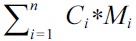
indicates the total latency of the DRAM accesses. Specifically,
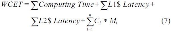
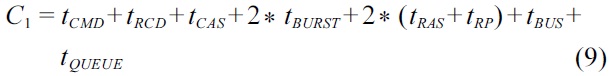
If there are N identical cores sharing the DRAM on a multicore processor, it will be safe but pessimistic to estimate the worst-case latency of each DRAM access based on two assumptions. The first assumption is that each DRAM access from a thread is always issued with other
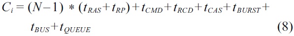
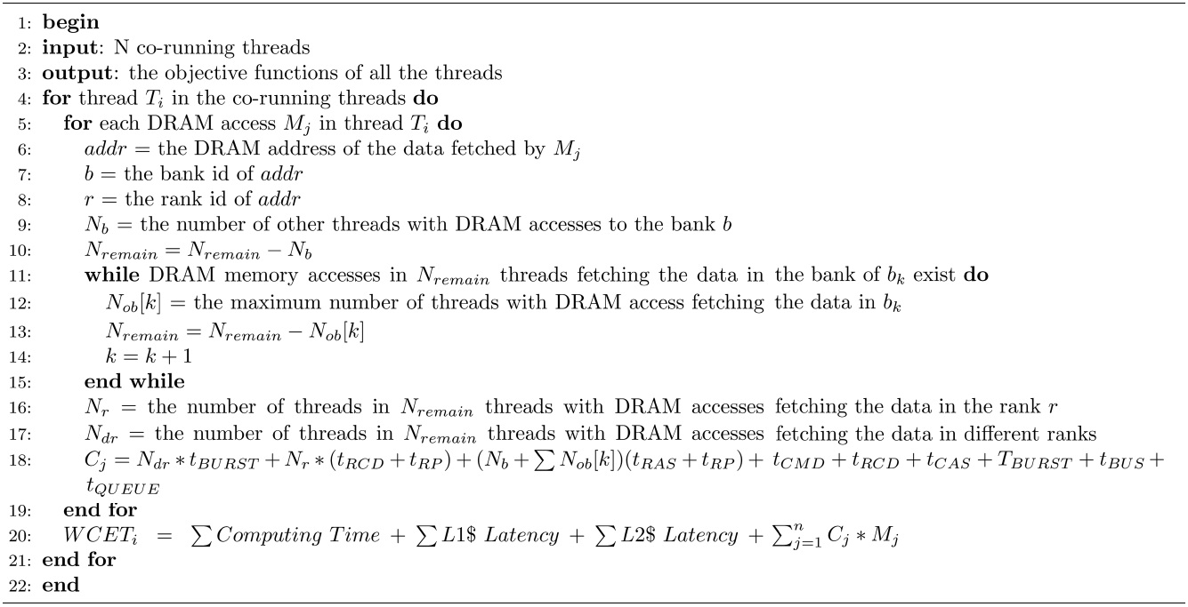
In order to reduce the overestimation in the conservative approach, the basic approach is proposed by considering the effect of DRAM command pipelining. As discussed in Section IV-C, the performance of DRAM command pipelining among consecutive DRAM accesses depends on the spatial locality of the data fetched. The worst-case situation of DRAM command pipelining happens when the data fetched by consecutive DRAM accesses are on the same bank, which would degrade the degree of DRAM command pipelining mostly. Given a thread (task), the basic approach first checks the DRAM address of the data fetched by each DRAM access. Then, it determines the maximum number of DRAM accesses from other threads fetching the data on the same bank with this access. If no DRAM access from other threads is found to fetch the data on the same bank, it then examines the number of DRAM accesses from other threads fetching the data on the same rank.
The basic approach is described in Algorithm 1. The input of this algorithm is N co-running threads, and the output is the WCET objective function of each thread. The worst-case DRAM performance of each co-running thread is estimated individually. The worst-case latency for a given DRAM access
>
C. An Example of the Basic Approach
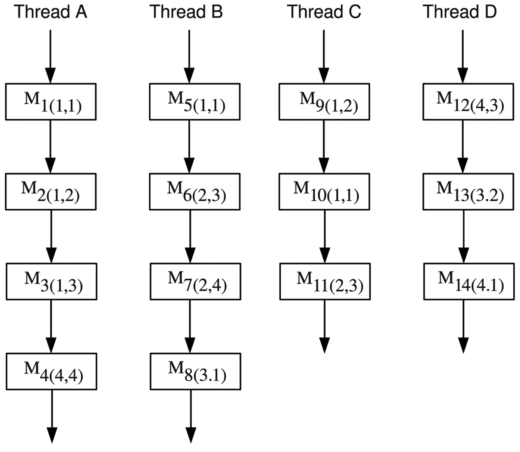
An example of the basic approach is shown in Fig. 6. In this example, there are 4 threads running concurrently on a multicore processor with 4 cores. In each thread, there are multiple DRAM accesses. It is supposed that there are 4 ranks in the DRAM of this example, and each rank has 4 banks. A DRAM access is represented by a rectangle with the name
The estimation procedure for
[Table 6] Algorithm 1 Basic Approach

Algorithm 1 Basic Approach
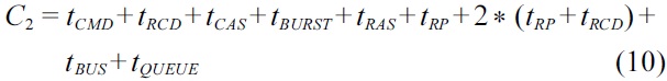
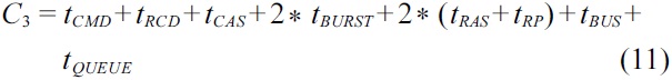
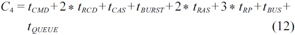
be calculated by Equation (10). This case is similar to the cases of
Following the specific timing parameters given in Table 2, the worst-case latency for
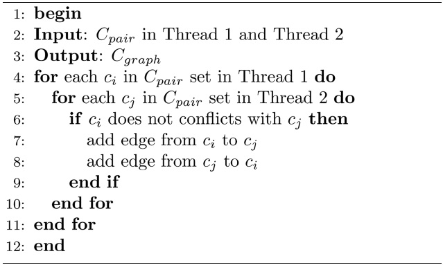
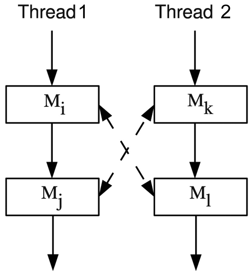
Although the basic approach considers the effect of DRAM command pipelining on the worst-case DRAM performance, there is still overestimation due to the timing order constraints of the co-running DRAM accesses, since the order of DRAM accesses of a given thread can impact the timing order of DRAM accesses of other threads. This problem can be explained by the example in Fig. 7. Assuming that there are two DRAM accesses in each thread, Thread 1 contains
An enhanced approach is proposed to compute the worst-case DRAM performance more accurately by eliminating the bank conflicts and rank conflicts that can never occur. A type of variables named
The construction of
In our evaluation, the simulation tool SimpleScalar [19] is extended to simulate the multicore architecture to obtain the simulated WCET. Also, the DRAM simulation tool named DRAMSim [20] is integrated into the extended SimpleScalar to support the accurate timing simulation of DRAM memory access. The WCET analysis tool consists of a front end and a back end. The front end of the WCET analysis tool compiles benchmarks into common object file format (COFF) binary code using the GCC compiler, which is targeted to SimpleScalar. Then, it obtains the global CFG and related information about the
[Table 7] Algorithm 2 Cgraph Construction

Algorithm 2 Cgraph Construction
[Table 8] Algorithm 3 V alid Cpair Set Construction
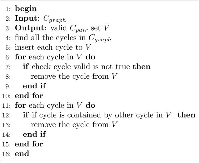
Algorithm 3 V alid Cpair Set Construction
instructions by disassembling the binary code generated. Subsequently, the back end compiler performs static cache analysis and the DRAM memory access timing analysis with the enhanced ILP method. Finally a commercial ILP solver, CPLEX [21], is used to solve the ILP problem to obtain the estimated WCET.
In our evaluation, a homogeneous multicore processor is simulated, and each core has an inclusive two-level
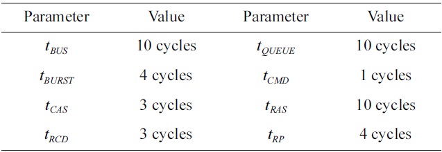
[Table 2.] Timing parameters of the DRAM memory

Timing parameters of the DRAM memory
[Table 3.] Basic configuration of the cache in the simulated processor
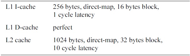
Basic configuration of the cache in the simulated processor
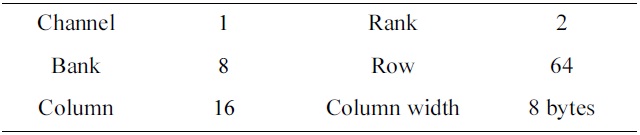
[Table 4.] Basic configuration of the DRAM memory

Basic configuration of the DRAM memory
cache [22]. The cache configuration in each core is described in Table 3. In order to focus on DRAM memory accesses from instruction accesses, the L1 data cache in each core is assumed to be perfect. The size of the shared DRAM memory between different cores in our evaluation architecture is 128 kbytes, and its configuration is shown in Table 4. The timing parameters of the DRAM memory are given in Table 2.
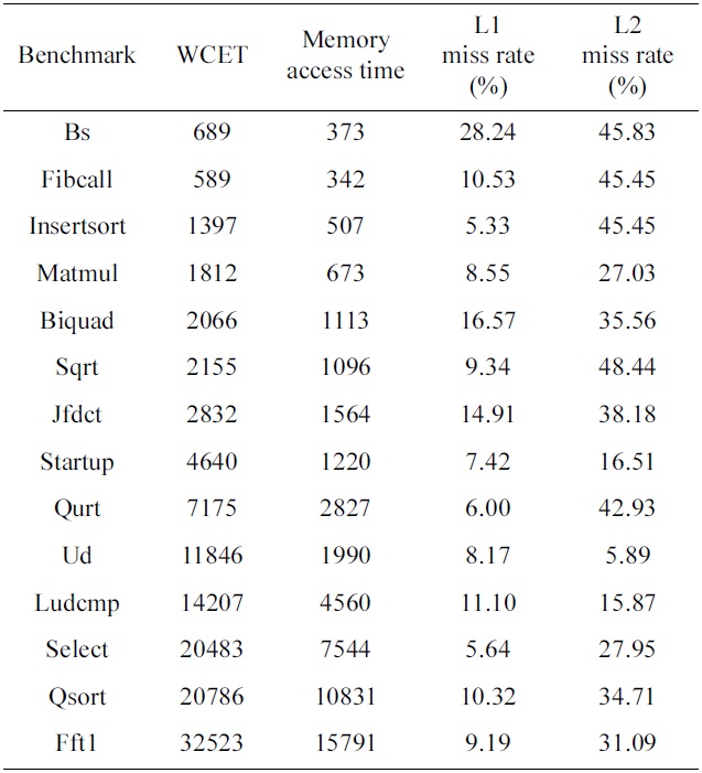
We use 14 benchmarks from the Malardalen WCET benchmark suite [23], and run them on processors with 2 cores, 4 cores, and 8 cores. The salient characteristics of the benchmarks can be found in Table 5. In our experiments, we study the following four schemes:
Conservative scheme: the WCET is computed by the conservative approach.
Basic scheme: the WCET is calculated by the basic approach.
Enhanced scheme: the WCET is derived by the enhanced approach.
Simulated scheme: the WCET is obtained by the simulation.
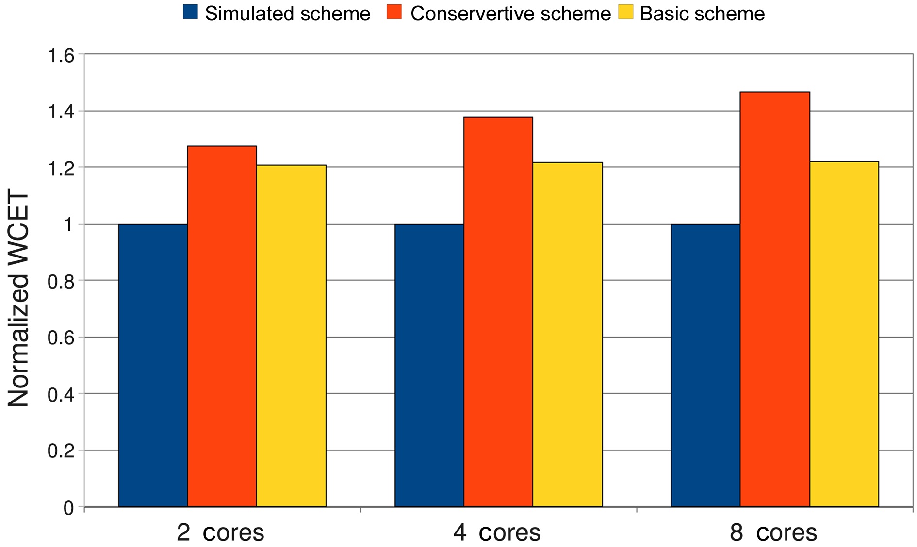
We first study the estimated WCET obtained by both the conservative approach and the basic approach in
[Table 5.] Salient characteristics of the benchmarks in case of 2 cores

Salient characteristics of the benchmarks in case of 2 cores
cases of 2 cores, 4 cores, and 8 cores. Fig. 8 demonstrates the averaged WCETs of the conservative scheme and the basic scheme, which are normalized with those of the simulated scheme in case of 2 cores, 4 cores, and 8 cores.
The overestimation of the conservative scheme, as compared to the simulated scheme, increases with the increase of the number of cores in the experiments. For 2 cores, the normalized WCET of the conservative scheme is 27.5% larger than that of the simulated scheme on average, and this difference increases to 37.5% and 46.7% for 4 cores and 8 cores, respectively. This can be explained by Equation (8) derived from the conservative
approach, where the number of cores
In contrast, the WCET differences between the basic scheme and the simulated scheme are much lower, at 20.7%, 21.8%, and 21.9% for 2 cores, 4 cores, and 8 cores, respectively. The reason for the lower overestimation is that the basic approach considers the effects of DRAM command pipelining among the consecutive DRAM accesses. The overestimation of the basic approach originates from the assumption that a given DRAM access is always executed after other co-running DRAM accesses, and from the ignorance of the timing order constraints of the co-running threads.
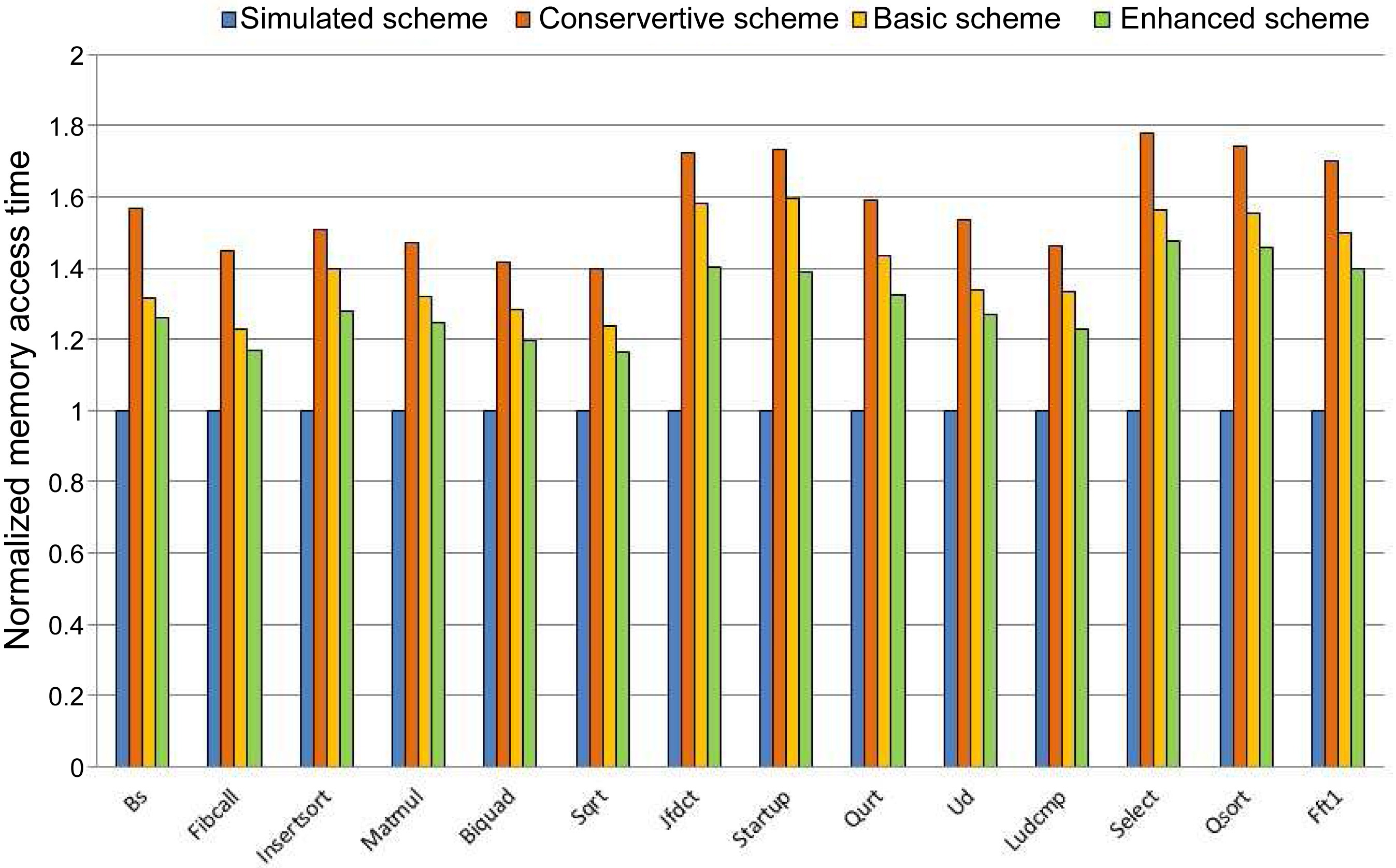
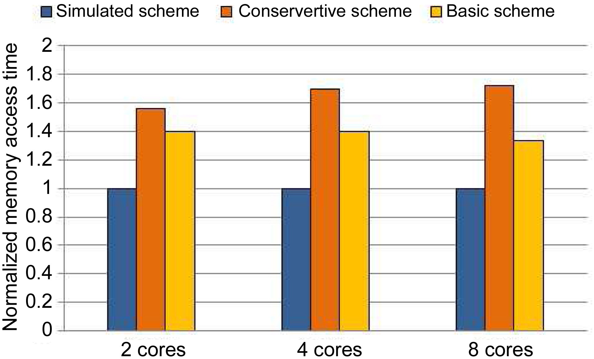
We also compare the memory access time of the conservative scheme, the basic scheme, and the simulated
scheme in Fig. 9. For the conservative scheme, the memory access time is overestimated by 56.3%, 69.8%, and 72.1% compared to the simulated scheme for 2 cores, 4 cores, and 8 cores, respectively. The Basic Scheme overestimates the memory access time by 39.9%, 39.7%, and 33.3% compared with the simulated scheme for 2 cores, 4 cores, and 8 cores, respectively.
>
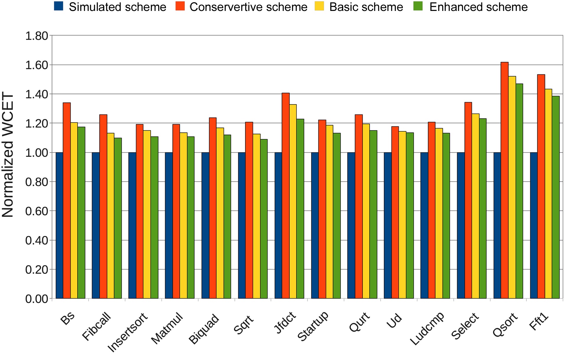
B. Results of Enhanced Scheme
Fig. 10 compares the WCETs of each benchmark for all four schemes. As expected, the enhanced scheme has the tightest WCET results, which are only 16.8% higher on average than that of the simulated WCET. The tighter WCET estimation is a result of the more accurate analysis of the memory access time. Fig. 11 shows the comparison of the memory access time of each benchmark for all
four schemes. Clearly, the enhanced scheme has the smallest overestimation, which is 30.4% on average. In contrast, the conservative approach and the basic approach result in 57.7% and 40.6% overestimation on average, respectively.
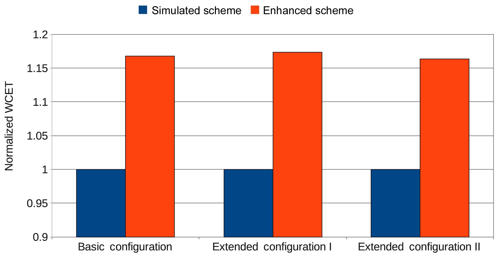
In addition, the basic configuration of the DRAM memory in our experiment is extended to two configurations by changing the number of the banks while keeping the total size of the DRAM the same. In extended configuration I, the number of banks is increased to 16, and the number of rows in each bank is reduced to 32. In contrast, the number of banks is decreased to 4, but the number of rows is increased to 128 in extended configuration II. Experiments are conducted for the Enhanced Scheme and the Simulated Scheme in these three DRAM configurations for 2 cores. Fig. 12 shows the comparison of the WCET of the enhanced scheme normalized with that of the simulated scheme in the basic configuration, extended configuration I, and extended configuration II for 2 cores. The estimated WCETs of the enhanced scheme are 16.8%, 17.3%, and 16.3% larger than those of the simulated scheme for the basic configuration, extended configuration I, and extended configuration II, respectively, indicating that the enhanced approach also works well with different numbers of banks.
We have address the difficulties in bounding the worstcase DRAM performance for a real-time application running on a multicore processor. The timing characteristics of DRAM accesses were investigated based on a generic DRAM access protocol, and it was found that the DRAM command pipelining of consecutive DRAM accesses can possibly impact the worst-case DRAM performance of a real-time application running on a multicore processor. A basic approach has been proposed for bounding the worstcase DRAM performance by considering the worst-case timing effects of DRAM command pipelining for the sequences of consecutive DRAM accesses. An enhanced approach has also been proposed for reducing the overestimation of DRAM access time by checking the timing order constraints of the co-running applications to identify and remove impossible DRAM access sequences.
Our experiments show that compared with the conservative approach, which assumes that no DRAM command pipelining exists, the basic approach can bound the WCET more tightly. For example, 15.7% improved performance was achieved on average for a 4-core processor. Moreover, the enhanced approach further improves the tightness of WCET by 4.2% on average compared with the basic approach.
In the future, our work will be extended to bound the worst-case DRAM performance with data DRAM accesses. The impact of the DRAM refresh on the WCET of a realtime application [24] will be integrated in future work.


![Command and data movement for an individual DRAM device access on a generic DRAM device [13].](http://oak.go.kr/repository/journal/11983/E1EIKI_2013_v7n1_53_f003.jpg)
![A cycle of a DRAM device access to read data [13].](http://oak.go.kr/repository/journal/11983/E1EIKI_2013_v7n1_53_f004.jpg)