P-type Si wafers were dipped in HF solution. The minority carrier lifetime (lifetime) increased after HF treatment due to the hydrogen termination effect. To investigate the film passivation effect, PECVD was used to deposit SiNx on both HF-treated and untreated wafers. SiNx generally helped to improve the lifetime. A thermal process at 850℃ reduced the lifetime of all wafers because of the dehydrogenation at high temperature. However, the HF-treated wafers showed better lifetime than untreated wafers. PERCs both passivated and not passivated by HF treatment were fabricated on the rear side, and their characteristics were measured. The short-circuit current density and the open-circuit voltage were improved due to the effectively increased lifetime by HF treatment.
In the crystalline solar cell industry, improving efficiency is of vital importance. Highly efficient solar cells require minimizing the loss of the carrier generated by the irradiation of light. This has made research on improving the minority carrier lifetime (lifetime) by surface passivation especially valuable for manufacturing highly efficient solar cells. Because of the thinning of the wafer, the lifetime improvement is required both the front and back side of the wafer. The back surface recombination velocity (BSRV) and back surface reflectance (BSR) of screen-printed full-Al back-contact cells are not effective to inhibit the loss of cell efficiency caused by reduced wafer thickness [1-4]. In order to solve this problem, passivated solar cells on the back surface, such as passivated emitter and rear cells (PERCs), have been studied by many research groups [3,4].
Decreasing defects of the wafer surface by passivation increases the lifetime. On a basic level, surface passivation can be divided into two methods. One is the chemical passivation method using a solution containing hydrofluoric acid (HF), iodine, etc. The other is thin film passivation using silicon oxide (SiO2), silicon nitride (Si3N4), etc. The HF treatment method has been found to be very useful for improving the lifetime through the hydrogen termination (H-termination) of the dangling bonds on the wafer surface [5-9].
The effect of HF treatment is widely known, but its application has not been sufficiently researched to improve the rear side passivation effect of PERCs. The chemical passivation by HF treatment was studied for the rear surface passivation of ptype Si-based crystalline solar cells. The HF treatment times and concentrations were adjusted to find the ideal combination. To confirm the change of the lifetime according to air exposure time, the HF-treated wafers were stored in air for a long time. A tube furnace was used to test the thermal stability of HF-treated wafers in the firing process. Finally, PERCs with HF treatment were fabricated. To compare the characteristics, untreated wafers were also prepared for each experiment.
Table 1 indicates the experimental order for testing the effect of HF treatment on the lifetime.
P-type Cz (Czochralski) silicon solar wafers with 200 ㎛ thickness and 78 ㎜ × 78 ㎜ area were used. Processes for saw damage removal (SDR) and RCA cleaning were performed to remove the damage, particles, and metal impurities on the wafer surface. SC-1 (an ammonia and peroxide mixture: APM, NH4OH:H2O2:H2O=1:2:7) and SC-2 (a hydrochloric acid and peroxide mixture: HPM, HCl:H2O2:H2O=1:2:8) were used for 10 minutes at 80℃. Diluted HF (DHF) was used for the HF treatment. The HF concentration ratio (HF:H2O=1:1, HF:H2O=1:10, HF:H2O=1:50) and treatment time (1~70s) were varied. The HFtreated wafers were exposed to air and the lifetime was measured. SiNx was deposited on HF-treated wafers to examine the effects on lifetime of film passivation. SiNx was deposited using plasma-enhanced chemical vapor deposition (PECVD). Silane (SiH4), ammonia (NH3), and nitrogen (N2) gases were used, and the substrate temperature was 400℃. The NH3/SiH4 ratio was 4, and the RF power was 600 W. The process pressure was 1 Torr. A tube furnace was used for heat treatment of the wafers at 850℃. After the thermal process, the lifetime of HF-treated wafers was compared with that of wafers untreated with HF. The hydrogen content of the interface was measured according to the thermal process through secondary ion mass spectrometry (SIMS) analysis. The lifetime was measured using microwave photoconductive decay (MW-PCD) equipment.
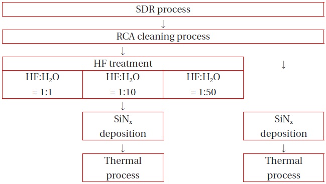
Table 2 shows the process order of PERC passivated by HF treatment on the rear surface.
P-type Cz silicon solar wafers with 200 ㎛ thickness and 78 ㎜ × 78 ㎜ area were used. A thick SiNx was deposited on the rear side by PECVD as a barrier to protect the surface during the surface texturing and phosphorus doping processes. A potassium hydroxide (KOH) solution was used for the front side surface texturing for 30 minutes. The n+ emitter layer was formed in thermal diffusion using the POCl3 tube furnace. A thick SiNx on the rear side was etched by plasma, and then a 100 ㎚ SiO2 was deposited on the front side of the wafer to protect the overall pyramid structure from SDR and RCA cleaning for the rear side. DHF (HF:H2O=1:10) solution was used to remove the overall phosphorus silicate glass (PSG) film and to reduce defects such as dangling bonds on the wafer surface. A 100 ㎚ SiNx was deposited as an anti-reflection coating (ARC) and for the rear side passivation. The rear side passivation film was locally opened for the electrode contact by a 532 ㎚ laser. Metallization was conducted using screen printing method. Ag paste was used as a front electrode, and Al paste was used as a rear electrode. A firing process was applied using a belt furnace, and then edge isolation was carried out using a 532 ㎚ laser equipment. Finally, the characteristics of the fabricated PERCs were evaluated.
3.1 The lifetime according to HF treatment times and concentrations
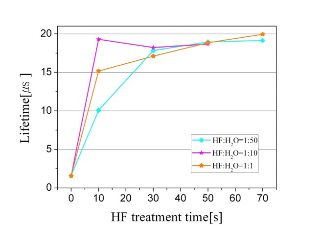
Figure 1 indicates the lifetime of HF-treated wafers according to the HF treatment times and concentrations. The lifetime of all wafers was increased by HF treatment. During the first several seconds, the lifetime of wafers increased randomly. However, regardless of the HF concentration, the lifetime of wafers became equal to about 18 ㎲ after about 50 seconds. From the results, it is anticipated that the chemical native SiO2 grown in RCA cleaning is etched by HF treatment during the first several seconds. Varied increase rates in the lifetime are shown because each wafer has a
[Table 1.] Process of experiment.
Process of experiment.
[Table 2.] Fabrication process of PERC.

Fabrication process of PERC.
different thickness of the native SiO2 grown in RCA cleaning [5-8]. Furthermore, the three DHF solutions have different expiration dates and HF concentrations. However, the lifetime of all wafers levels out after about 50 seconds without the HF concentration, because the H-termination that negates the defects reaches a saturation point. Therefore, in all subsequent experiments, DHF (HF:H2O=1:10) solution was applied for 50 seconds.
3.2 The lifetime according to air exposure time
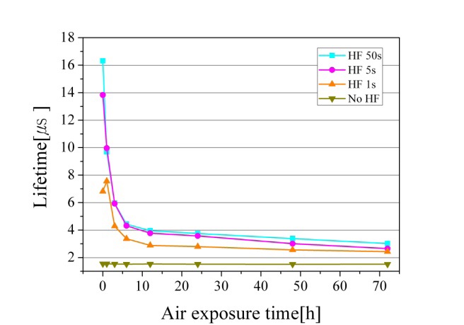
Figure 2 indicates the lifetime of HF-treated wafers according to air exposure time in a clean room atmosphere. The HF (HF:H2O=1:10) treatment time was varied.
For the first 24 hours, the lifetime of all wafers decreased differently according to the HF treatment times, except for the untreated wafer. After 70 hours of exposure, the lifetime of all wafers was fixed at about 2.5 ㎲. It is thought that the lifetime decreases over about 10 hours because of rapid native SiO2 growth by composite effects including dehydrogenation, Si density of the surface, adsorbents like carbon and oxygen, and dangling bonds, etc. After about 10 hours, it is considered to grow the
3.3 Effects of the SiNx deposition on the lifetime
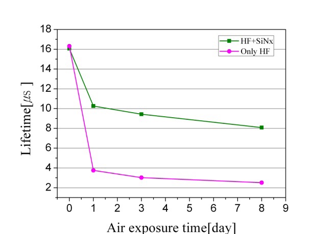
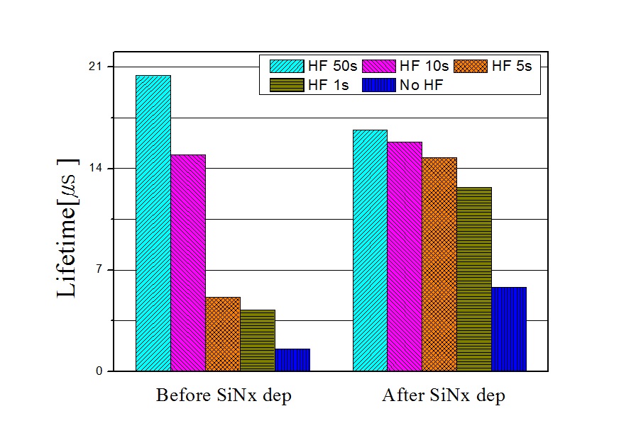
Figure 3 shows the lifetime of wafers on which a 100 ㎚ SiNx was deposited after HF (HF:H2O=1:10, 50) treatment, according to air exposure time in the clean room atmosphere.
The lifetime of wafers without SiNx decreased to about 4 ㎲ in 24 hours. However, the lifetime of wafers with SiNx was reduced somewhat compared to wafers without SiNx. From the figure, it is considered that when SiNx is deposited on HF-treated wafers, the wafers are protected against the aforementioned composite effects.
Figure 4 indicates the lifetime of wafers with various HF (HF:H2O=1:10) treatment times according to the 100 ㎚ SiNx deposition. The HF treatment times were adjusted to 0, 1, 5, 10, 50 seconds.
With the SiNx deposition, the lifetime of wafers HF-treated for a short time increased more than those of wafers HF-treated for a long time. However, the lifetime of wafers HF-treated for 50 seconds decreased from 20.41 ㎲ to 16.68 ㎲ due to the SiNx deposition. It is expected that when the wafers are shortly treated by HF, the remaining defects are reduced by the passivation effect of the SiNx deposition [10,11]. However, when the H-termination becomes saturated with HF treatment for 50 seconds, the stress of SiNx deposited by PECVD can reduce the lifetime [12]. Nevertheless, it is clear that the lifetime of wafers HF-treated for 50 seconds with the SiNx deposition achieves the best result.
Two passivation effects of SiNx on p-type wafers are expected: the reduction of the dangling bonds at the interface by atomic hydrogen, and the field-effect passivation caused by a high density of fixed positive charges. The stress effect that is detrimental to the electrical and optical performance of devices is also considered. It is thought that when the lifetime of wafers treated with HF for a short time is very low, the passivation effects of SiNx are more pronounced than the stress effect. However, when
the lifetime of wafers is very high, the stress effect is much higher compared with the passivation effects, which decreases the lifetime.
3.4 The lifetime according to the thermal process
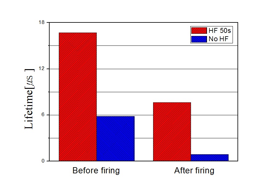
Figure 5 indicates the lifetime of HF-treated wafers according to the thermal process at 850℃. Before the thermal process, the HF treatment (HF:H2O=1:10, 50s) was applied and a 100 ㎚ SiNx was deposited.
The lifetime of all wafers decreased after the thermal process.
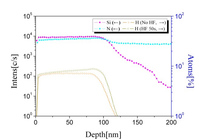
Figure 6 shows the hydrogen content of HF-treated wafers according to the thermal process at 850℃. A 100 ㎚ SiNx was deposited before the thermal process. The dehydrogenation in the interface between the wafer and SiNx was investigated after the thermal process.
It is considered that the lifetime is reduced from 16.68 ㎲ to 7.61 ㎲ in Fig. 5 because the hydrogen atoms probably effuse from the wafer.
Figure 7 signifies the hydrogen content of HF-treated wafer according to the thermal process at 850℃. A 100 ㎚ SiNx was deposited before the thermal process. To compare the hydrogen content after the thermal process, an untreated wafer was prepared. The hydrogen content in the interface (80-90 ㎚) of HFtreated wafer was higher than that of HF-untreated wafer after the thermal process.
From the results, it is anticipated that the lifetime of HFtreated wafer in Fig. 5 is higher than that of HF-untreated wafer, because the greater amount of hydrogen atoms in the interface led to a reduction in defects. Therefore, the lifetime of HF-treated wafers are found to be higher than those of HF-untreated wafers.
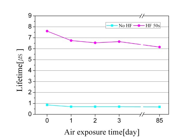
Figure 8 indicates the lifetime after the thermal process at 850℃ according to air exposure time. The lifetime of all wafers were reduced. The lifetime of the HF-treated wafers were reduced to about 6 ㎲ after 85 days. However, the lifetime was still
very higher than those of HF-untreated wafers.
3.5 PERCs characteristics according to HF treatment
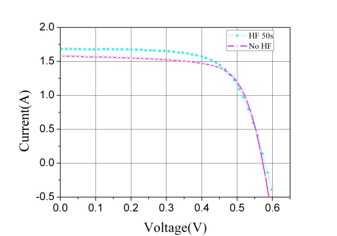
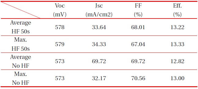
Table 3 shows the characteristics of fabricated PERCs according to HF treatment. Figure 9 I-V characteristic curve.
The efficiency of HF-treated PERCs was 13.22% on average, and the efficiency of untreated PERCs was 12.82% on average. The short-circuit current density (Jsc) and the open circuit voltage (Voc) of HF-treated PERCs was higher at 1.57 mA/cm2 and 5 mV on average than those of PERCs not treated with HF. It is thought that Jsc and Voc are increased because of the enhanced collection probability of the carriers and the decreased recombination of electron hole pairs (EHPs) in the interface between the rear surface and SiNx by the rear side passivation with HF treatment, which increased efficiency [1,2]. The efficiency of PERCs passivated
[Table 3.] PERC characteristics.
PERC characteristics.
by HF treatment is higher than that of the non-passivated PERCs. However, the efficiencies of PERCs were low in general because the PERC fabrication process was very complicated. The contact area on the rear side was just 1%, and the firing temperature and speed were set for standard solar cell fabrication. Also, all wafers were exposed many times to air, because the fabrication process was very complicated. Therefore, it is considered that the efficiency will be improved by greater optimization of the PERC fabrication process.
This research attempted to identify improvements in crystalline silicon solar cell efficiency by improving the rear side passivation characteristics using a chemical HF treatment method on p-type silicon wafers. PERCs were fabricated with HF treatment on the rear side of the wafer to measure the efficiency.
After HF treatment of 50 seconds, the lifetime had a fixed value of about 18 ㎲ irrespective of the HF concentration. When SiNx was deposited on the wafers, the decrease rate of the lifetimes according to air exposure time was reduced because SiNx protected the wafers from the composite effects including the native SiO2 growth, dehydrogenation, Si density of the surface, adsorbents like carbon and oxygen, and dangling bonds. In addition, after the thermal process at 850℃ for about 5 seconds, the lifetime of wafers with HF treatment and the SiNx deposition was reduced from 16.68 ㎲ to 7.6 ㎲. However, the lifetime of HF-treated wafers was still high compared with those of HF-untreated wafers after the thermal process, because of the greater abundance of hydrogen atoms in the interface.
The efficiency of PERCs passivated on the rear surface by HF treatment was 13.22%, higher than the 12.82% of the nonpassivated PERCs, because the carrier collection probability that was increased by HF treatment also made Jsc and Voc increase. However, the characteristics of solar cells were poor because all of the fabrication processes were not optimized. So, it is considered that the efficiency will be improved by greater optimization of the PERC fabrication process.