As an oxide semiconductor, ZnO has attracted considerable attention for its versatile application in electronics and optoelectronics devices due to its direct, wide band gap (3.4 eV), and high exciton binding energy (60 mV) at room temperature. These unique characteristics of ZnO have recently been studied for light emitter diode (LED), short wavelength, and UV laser diode (LD) in solar cells [1-5]. Especially, as a one-dimensional structure, ZnO nanowires have also been studied for their application in smaller size and high density devices. Useful properties of nanowires including a high surface to volume ratio have been investigated with the application of chemical and bio sensing devices [6-8]. ZnO is naturally an n-type semiconductor due to its inherent defects, such as Zn interstitials and oxygen vacancies [9]. However, the characteristic can vary from insulator to conducting properties by using various fabricating process such as growth condition or doping control [10-12]. The growth of nanowire has been explored by using various methods and mechanisms such as the vapor-phase transport process, chemical vapor deposition, pulsed laser deposition by using vapor-solid (VS) or vapor-liquid-solid (VLS) mechanism, and solution process [13-15]. Among them, the VLS mechanism is preferential for nanowire growth. This is because the nanowire growth process from a liquid catalyst proceeds from 10 to 100 times more rapidly than the growth process from a solid buffer layer [16]. Moreover, it is relatively easy to control the size of the nanowire diameter. Also, the electrical and optical properties of the nanowire are strongly dependent on the size of the nanowire diameter because of the surface and confinement effects [17-21]. It is important to control the size of the nanowire diameter systematically for device application. Michael et al. and Xing et al. previously reported that the diameter difference of ZnO and Si nanowire was controlled as adjusting the Au catalyst film thickness on the substrate [22,23]. Recently, Lee et al. reported the stimulated emission properties of diameter controlled ZnO nanowires using a buffer structure in a VS mechanism [24]. Nevertheless, the electrical properties of nanowire are still being challenged with the diameter controlled nanowire for the logic circuit of a device.
In this letter, we reported electrical transfer characteristics depending on different diameters of ZnO nanowires. ZnO nanowires were synthesized by using physical vapor deposition as VLS method. In order to control the size of the ZnO nanowire diameter, we simply changed the thickness of the Au catalyst on the substrate. We confirmed that the diameters of the ZnO nanowires were controlled by changing the thickness difference of the Au catalyst on the substrate. All ZnO nanowires have a single crystalline form and a number of defects. At an electrical transfer measurement of ZnO nanowires, we confirmed that different diameters of ZnO nanowire occur with the shift of threshold voltage (Vth).
ZnO nanowires were synthesized by using hot-walled pulsed laser deposition (HW-PLD). In order to control the diameter of ZnO nanowires, different thicknesses of Au catalyst film on c-plane sapphire substrates were deposited by using thermal evaporation. The detailed growth processes of ZnO nanowires have been reported previously [25]. The mixed nanowire solution of both fabricated ZnO nanowires and isopropyl alcohol was dispersed on the SiO2/Si substrates in order to fabricate ZnO nanowire field effect transistors (NW FETs). The electrodes of ZnO NW FETs were deposited by using e-beam evaporation and thermal evaporation with Ti (10 nm) and Au (200 nm), respectively. The NW FETs were patterned by using a conventional photo-lithography process. The morphology and crystalline characteristics of fabricated ZnO nanowires were analyzed using a field effect scanning electron microscope (FE-SEM) for high resolution transmission electron microscopy (HR-TEM).. The electrical properties of ZnO NW FETs were measured using a semiconductor parameter analyzer.
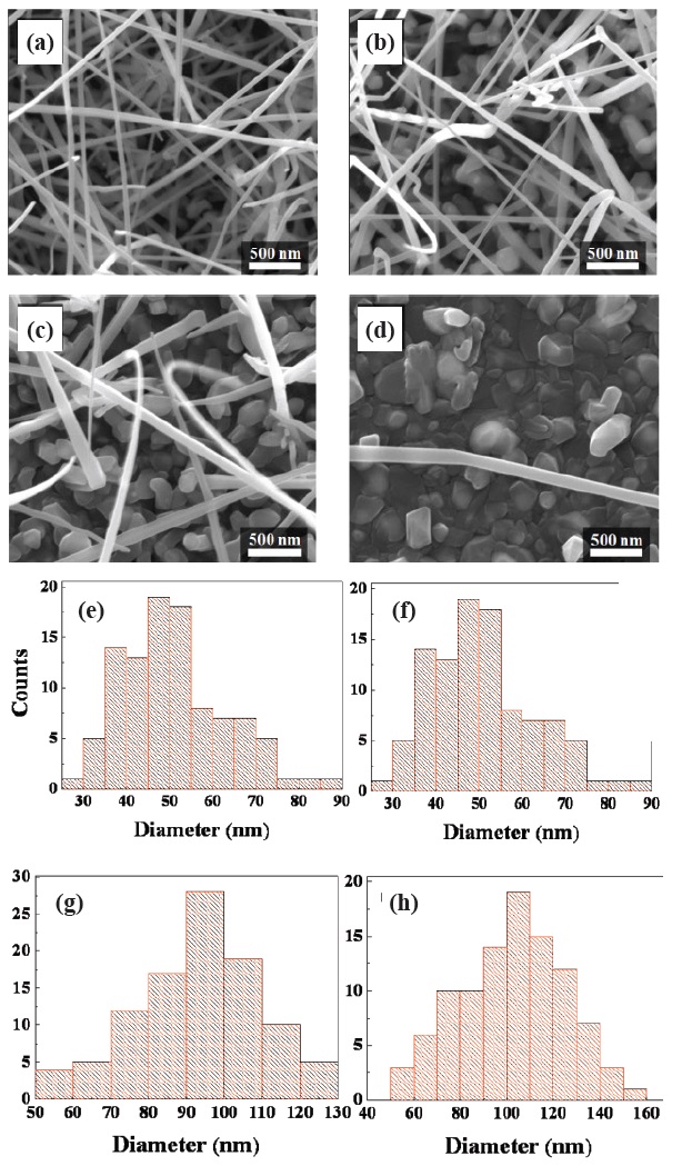
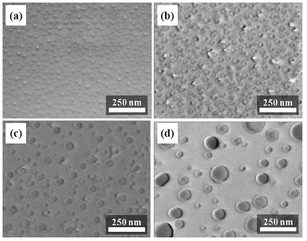
Figure 1 shows FE-SEM images of as-grown ZnO nanowires grown on sapphire substrates coated with 1 nm (a), 3 nm (b), 5 nm (c), and 7 nm (d) Au catalysts, and histograms of the measured diameters for the nanowires grown on a substrate coated with 1 nm (e), 3 nm (f), 5 nm (g), and 7 nm (h) Au catalyst films. As shown in Figs. 1 (a), (b), (c), and (d), Au particles were observed on the tips of the ZnO nanowires. These results clearly indicate that the ZnO nanowires were grown by a vapor-liquidsolid (VLS) mechanism. As shown in Figs. 1 (e), (f ), (g), and (h), the average diameters of ZnO nanowires were 64.3 nm, 88 nm, 112.4 nm, and 137.5 nm grown on substrates coated with 1 nm, 3 nm, 5 nm, and 7 nm Au catalyst films, respectively. The length of ZnO nanowires ranged from about 8 to 12 μm. The density of the ZnO nanowires decreased when the Au catalyst thickness was increased. Based on these results, it has been observed that the size of the Au droplet increased gradually as the Au catalyst thickness on the substrate increased, while the Au droplet formed into a larger sphere shape with a wide gap between other Au droplets. Due to the big size of the Au droplet from the thick Au catalyst, it is generally easy for it to form with adjacent droplets. Figure 2 shows the behavior of Au droplet clusters melted from 1 nm (a), 3 nm (b), 5 nm (c), and 7 nm (d) Au catalysts at 800℃ for 30 minutes. It is clearly observed that the size of the Au droplet is closely
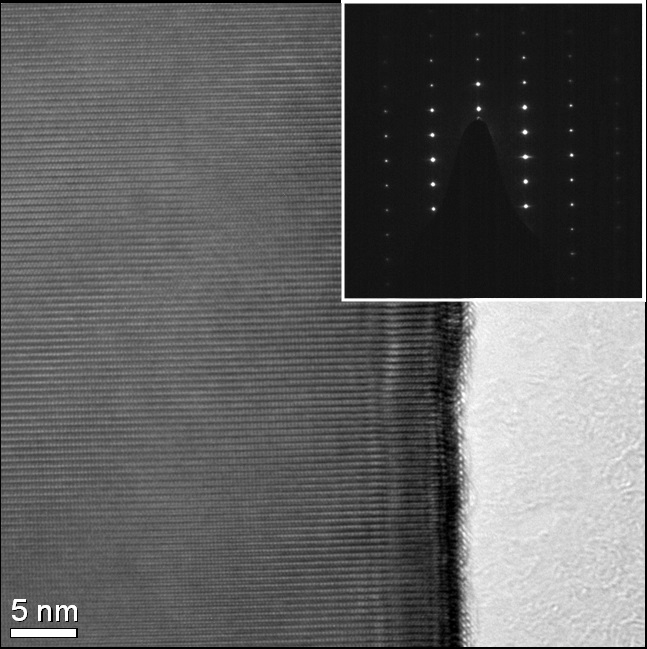
related to the thickness of the Au catalyst. Figure 3 shows a TEM image of a ZnO nanowire coated 2 nm Au catalyst on a substrate. The crystalline form of the ZnO nanowires grows in the (0001) direction. We confirmed that all ZnO nanowires have a single crystalline form by using a SEAD pattern. All ZnO nanowires showed good single crystalline form without any defects.
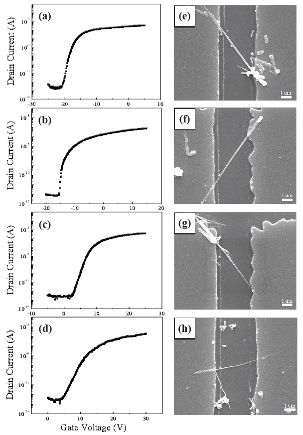
In order to analyze the electrical properties of ZnO NW FETs, we measured ZnO NW FETs using a semiconductor parameter analyzer at an ambient air condition. Figure 4 shows the electrical transfer curve of ZnO NW FETs with 98 nm (a), 80 nm (b), 70 nm (c), and 45 nm (d) diameters and FE-SEM images of ZnO NW FETs with 98 nm (e), 80 nm (f), 70 nm (g), and 45 nm (h) diameters, respectively. The Ion/off of ZnO NW FETs was 106 - 107. When the diameter size of the ZnO nanowire increases, Vth shifted in the negative direction. At 45 nm and 70 nm, the ZnO NW FETs have positive threshold voltages of 11.25 V and 0.85 V, respectively, defined as the enhancement mode with an off-current status at a zero gate bias. In contrast, at 80 nm and 98 nm, ZnO NW FETs have clear negative threshold voltages of -13.7 V and -23.7 V, respectively, defined as the depletion mode that exhibits the on current at the zero gate bias.
The Vth shift of ZnO NW FETs for different nanowire diameter sizes is related to the difference of the depletion region due to the different diameters of ZnO nanowires, which change the total number of carriers and trapped electrons. Because of the roughness difference of the ZnO nanowire, the Vth nanowire was changed due to the difference in the depletion region as reported by Hong et al. [26] At a small diameter, the depletion region is relatively large due to the increase in the trap density effect. This result induces a decrease in the current flow with zero bias. Therefore, ZnO nanowires with small diameter showed positive Vth, indicating that a more positive bias is needed to create the current path. On the other hand, at a large diameter, the effect of trap density is decreased because of the relatively small depletion region. From this result, Vth indicates that a more negative bias is required to deplete the carriers in the ZnO nanowire to the conductance layer. The nanowire can also modulate the transfer of free carriers, depending on the difference of nanowire diameter, resulting in a change of the total volume of channel layers. Thus, a higher bias voltage is required to turn on the ZnO nanowires with a smaller diameter of nanowires than that of the larger diameter nanowires. Since most nanowire FETs have almost the same carrier concentration of about 1017 /cm-3, the shift of threshold voltage showed strong diameter dependence, which is mainly due to the change of the number of free carriers in the active channel layer. This agrees well with the case of thin film transistors reported by Park et al. Park et al. reported that the number of free carriers in an active channel layer of ZnO based TFTs was proportional to the thickness of the active channel layer [27].
In summary, we have showed that the diameter of ZnO nanowires can be changed simply by adopting various Au catalyst thicknesses from 1 nm to 7 nm. All ZnO nanowires have a good crystalline form and (0001) growth direction. We demonstrated that controlling the diameter of ZnO nanowires provides a simple and efficient way for the Vth control of various ranges from enhanced mode to depleted mode in ZnO NW FETs systematically, and that the electrical transfer properties of ZnO nanowires between enhanced mode and depletion mode can be used as an advantage for device fabrication, such as nanowire inverters and logic circuits in terms of simplicity.