ABS has been used extensively for electrical and electronic applications due to its good mechanical properties and easy processing. Especially in the electronics industry, the need for polymer plates or films coated with metallic films, like printed circuit boards (PCBs), is growing. Light composite material with simultaneous metallic and ABS plastic properties might be obtained by plating ABS with a certain thickness of metal. However, most plastic materials cannot be plated by electroplating since they are nonconductive.
There are several methods for plating insulators and achieving required adhesion strength. Metallic films can be deposited on plastics by sputtering or evaporating metal in a vacuum chamber [1,2], which are physical coating methods. In chemical vapor deposition (CVD), metallic film on a substrate can be obtained by pyrolysis of metalorganic vapor in a chamber [1,2]. Metal can also be coated onto a nonconductive surface in an aqueous solution. A catalyst can reduce metallic ions into metal, forming metal film on a plastic surface, which is called electroless plating.
It is necessary to use a chamber system for sputtering, thermal evaporation, and CVD. Hence, the size of the product might be limited due to the size of the chamber. These methods also have low productivity and high cost in comparison with electroless plating because of their chamber systems. Another common yet crucial problem of these methods also occurs in that the binding between a metal film and substrate is weak. However, this problem can be solved in several ways, which depend on the plating methods and conditions. As an example, to increase the adhesion strength of metal on a substrate in sputtering, a strong adhesive metallic buffer layer of Ti or Cr can be coated prior to the metal deposition process. In electroless plating, the surface of a substrate can be etched or modified before the metal plating process, forming holes or ditches that anchor the plated metal, so that the binding of the metal film to the substrate is strengthened considerably [3].
Strongly acidic chemicals such as dichromic acid, fluoridationhydrogen acid, and hydrochloric acid have usually been used in etching processes to produce anchoring sites on polymeric plastics [4], which has caused environmental problems. The etching conditions and chemicals used differ from polymer to polymer [3].
Environmentally friendly techniques for modifying or etching polymeric surfaces have been developed, but have not yet been proven to be effective for industrial uses [5-9]. We have performed surface modification using plasma prior to electroless Ni plating as an etching process for ABS surfaces. This method was successfully applied to electroless Ni plating on polypropylene (PP) [10]. Plasma was generated in air at atmospheric pressure with DBDs [11]. The process is environmentally friendly, especially with regard to water pollution problems, and can be applied simply to industry. After the surfaces were etched or modified, the static contact angles were measured to observe the hydrophilicity of the surfaces, and surface images were taken using SEM. To examine the adhesion strength of metal film on ABS, cross-sectional SEM images were taken. Cross-cutting and peeloff tests with 3M tape [10], 90° peel-off tests, and thermal shock tests were also performed.
All results from the treated specimens were compared with those from chemically etched specimens. The results reveal that the developed technique is reliable for the modification and etching of ABS surfaces for electroless plating.
Commercially available ABS plate with a thickness of 1.0 mm was cut to a size of approximately 100 mm × 50 mm for plasma treatment preparation.In the chemical etching and electroless plating processes, hot plates were used to control the temperature of the solution, and magnetic stirrers were used to keep the temperature constant throughout the volume of the solution. Prior to chemical etching, a 24-kHz ultra-sonic cleaner was used for degreasing the ABS surface. Electroplating was performed in a constant-temperature water bath with water circulation. Contact angles were measured using DI water droplets.
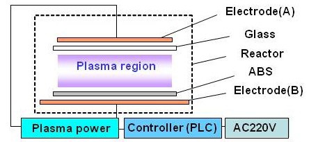
The custom-built plasma etching system is composed of three parts: a reactor in which plasma production and surface modification occur, a high-voltage power supply for plasma generation, and a controller. The controller regulates the power input to the reactor according to programmed instruction sequences from a computer interface. The controller consists of solid-state relays and a programmable logic controller (PLC). The plasma power supply provides an output peak voltage of 15 kV and a maximum alternating current (AC) of 100 mA with a 20-kHz square wave. Figure 1 shows a schematic configuration of the plasma etching system. 2-mm-thick commercial glass sheet was used as the dielectric barrier. 2-mm-thick commercial copper plates were used as high-thermal-conductivity electrodes. No matching box was used between the plasma power supply and the reactor. The reactor was operated at atmospheric pressure in air, and the system was kept in open space at room temperature. Niclekl (Ni) was chosen as a plating metal for convenience. The temperature of the reactor during its operation was monitored using an infrared thermometer.
2.2 Sample preparations and surface modifications
For good electroless plating, the ABS surface has to be hydrophilic. Even if there is a sufficient number of anchor sites on the surface, metal should be evenly coated in holes or anchor sites to obtain the required binding strength. Hence, it is necessary to transform the ABS surface from hydrophobic to hydrophilic. In chemical etching, the hydrophilicity is altered by acidic treatment, but in plasma treatment, it is changed by plasma irradiation.
For the chemical etching, physical adsorbates were removed, and degreasing was done with sonication for 3 minutes at 50℃ in a water bath. Release agent on the ABS surface usually prevents water from contacting the ABS surface, it must be removed using a surfactant solution before the chemical etching process. Then, chemical etching was done in an etching solution with a composition of (CrO3 380 g + H2SO4 370 g)/l at 65℃. The etching times ranged from 30 s to 210 s.
For plasma treatment, ABS samples were firstly washed with tap water to remove physical adsorbates on the surfaces, and then dried before plasma treatment. It was not necessary to degrease the surfaces of samples prior to treatment, because the plasma can simultaneously modify and degrease the surfaces.
After investigating uniformity of the surface treated by plasma, the sample size was determined for plasma treatment. On top of the lower electrode, dry samples were placed as shown in Fig. 1, so that only the top sides were treated by plasma. The bottom sides were placed close to the electrode to prevent modification by plasma.
ABS is a thermoplastic polymer, and continuous operation of an atmospheric DBD plasma system usually generates heat that might be high enough to give rise to irreversible deformation of the ABS. So, to avoid this thermal deformation of ABS, the reactor was operated in discontinuous way. The optimal timing sequence was established by preliminary experiments. DBDs generated plasma at atmospheric pressure. The reactor was air-cooled and kept in ambient conditions, and during operation, its temperature rose to 50℃, far below the melting temperature of ABS. The plasma system consumed about 70 W during operation.
The total plasma treatment times were in a range of 30 s~180 s,
which was chosen in preliminary experiments to match the numbers of anchor sites with those obtained by chemical etching.
An electroless Ni plating process was begun within a minute after the completion of the surface modification process. The process consists of the following steps: (1) Neutralization with 10% HCl at room temperature for 1 min, followed by rinsing with DI water for 30 s to obtain uniform metal plating on the modified surfaces by making the surfaces active and by removing residues. (2) Conditioning with H3BO3 11% + KOH 5% + H3NO3S 10% + DI water 74% at 45℃ for 5 minutes, then rinsing with DI water for 30 s to allow metallic ions to permeate well into anchor sites or holes. (3) Pre-dipping with 200 g of (NaCl 98% + C6H8O73K 2%) + 1 liter of DI water at room temperature for 1 minute for the stable and uniform adsorption of catalyst on the modified ABS surfaces. (4) Catalyzing with 10 ml of (HCl 38% + SnCl2 42% + PdCl2 1% + DI water 19%) + 200 g of (NaCl 98% + C6H8O73K 2%) + 990 ml of DI water at 50℃ for 5 minutes, then rinsing with DI water for 30 s. As a core process in electroless plating, this is done to allow PdCl2 to be adsorbed on the modified surfaces. The adsorbed Pd will initiate the reduction of metallic ions. (5) Acceleration with 10 g of (NaCl 1.4% + CH2O3Na 98.6%) + 10 ml of (Na2ClO 32% + DI water 68%) + 990 ml of DI water at 50℃ for 1 minute, then rinsing with DI water for 30 s. This step is to remove the Sn included in palladium colloid after catalyzing. (6) Electroless Ni plating with 100 ml of (NiSO47H2O 32.5% + CH3CH(OH)COOH 3.5% + DI water 64%) + 100 ml of (NaH2PO2H2O 20% + C4H6O5 5% + DI water 75%) + 800 ml of DI water at 88℃ for 5 minutes. The electroless Ni plating solution is composed of Ni salt, reducing agent, and a buffer solution and pH adjuster as additives. Dipping the processed ABS into this solution, Ni ions are reduced by Pd on the ABS surface, and then become Ni metal. The thickness of the Ni film is proportional to the dipping time. But if the dipping time is too long, defects and stains appear unavoidably on the plated surface. Therefore, a proper dipping time must be chosen in advance to achieve the recommended Ni thickness, which is about 0.2~0.5 μm.
Electro Ni plating is necessary for the adhesion strength tests of Ni films on ABS to check whether test results meet industrial standards. For the 90° peel-off test, the coated metal film should have enough tensile strength. For this purpose, a relatively thick additional Ni layer (~20 μm) on the electroless Ni plating surface is needed. Ni electroplating was done for both the plasma-treated and the chemically etched samples in a solution containing 500 ml of Ni(NH2SO3)24H2O + 25 g of NiCl26H2O + 45 g of H3BO3 + 500 ml of DI water at 45℃ for 40 minutes with a current density of 20 mA/cm2. The time and the current density for electroplating were determined by the sample size and the plating thickness.
2.4 Measurement and observation
Because electroless plating occurs in a solution, in order to have uniform Ni plating, the modified surface has to be hydrophilic, so that the plating solution permeates into the holes or ditches on the surface. The hydrophilicity of the sample surfaces before and after the plasma modification and the chemical etching was examined by measuring static contact angles with DIwater droplets. Plasma treatment is a dry process, and electro plating is a wet process. So, there is a time interval between these two processes within which the sample is transferred from one process to the other, and during which the hydrophilicity might be changed. If the hydrophilicity depends on the time interval, the binding characteristics of plated Ni would also depend on the time interval. Therefore, it was necessary to know how contact angles would change as exposure time to air changes after the plasma-induced surface modification process. For comparison, the contact angles of chemically etched samples were also measured. The measured values were averaged out after five measurements, and the errors were within ±5°.
The physical binding of metal to ABS is important for good adhesion strength, so the shapes of holes or anchor sites on the sample surfaces are just as important. Before and after the etching (or the modification) processes, the surfaces were observed with field emission SEM to examine the surface morphologies of the samples. After the plating processes, cross-sectional SEM images were taken in order to see whether the insides of the holes or the anchor sites were coated with Ni. ABS plastic at a temperature around that of liquid nitrogen is so brittle that it is easy to break by a proper mechanical impact. The cross sections of Niplated samples were made by applying a mechanical impact with a mechanical tool in a short period of time, after dipping the Niplated samples into liquid nitrogen, where they were held for a while to achieve thermal equilibrium, and then pulling them out quickly. The procedure for creating these cross sections is known as the freeze-fracture method.
In order to investigate the adhesion strength of metal film on the ABS surface, cross-cutting and peel-off tests with 3M tape (3M 810D standard) [9] and 90° peel-off tests were conducted. The test with 3M tape was done after making perpendicular crosscutting lines spaced approximately 1 mm on the plated surfaces with a sharp cutting tool. The forces to peel off the plated metal films from the sample surfaces were measured for the 90° peeloff test, in which metal films with 1-cm width were pulled at 90° from the sample surface.
The characteristics of metallic films and plastics differ in many respects. Therefore, it might be possible that the metallic film can be detached from a plated plastic surface depending on the circumstances in which it is used. As mentioned, separation tests by mechanical forces were done. Thermal stress tests were also carried out for at least 100 cycles, in order to verify that the adhesion strength of the Ni film on ABS upon sudden and great changes in temperature was satisfactory. One cycle of the thermal stress test involves dipping a plated sample quickly into liquid nitrogen, waiting for thermal equilibrium for minutes, pulling out the sample quickly from the liquid nitrogen, dipping into hot boiling water quickly, and waiting for thermal equilibrium for minutes.
The surfaces obtained by electroless plating followed by electroplating on the plasma-treated and chemically etched samples appeared to be shiny. As can be expected, the plated Ni film on the surface neither treated by plasma nor etched by chemicals was peeled off easily.
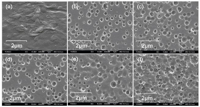
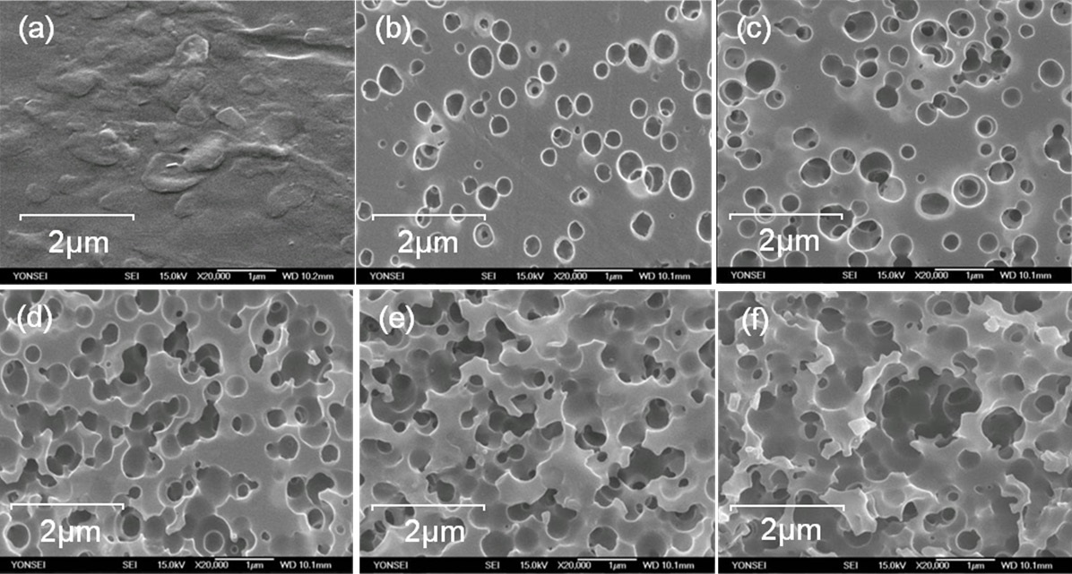
SEM images of the ABS surfaces subjected to chemical etching are shown in Fig. 2-1. Fig. 2-1(a) exhibits an SEM image of a bare
ABS surface. When the etching time was 30 s, holes were created by the etching with an approximate average size of 0.3 μm. As the etching time increased, the size and number of holes increased, such that holes with a size of approximately 1 μm could be found. Holes within holes were even created as the etching time increased. These holes were places occupied by butadiene in ABS, which was chemically etched out by strong acids. The holes provide anchoring sites for metal on the ABS.
Figure 2-2 shows SEM images of the surfaces modified by plasma treatment. The size of holes was not notably proportional to the plasma treatment time, but the number of holes was increased slightly with increasing plasma treatment time. The average size of holes was about 0.5 μm.
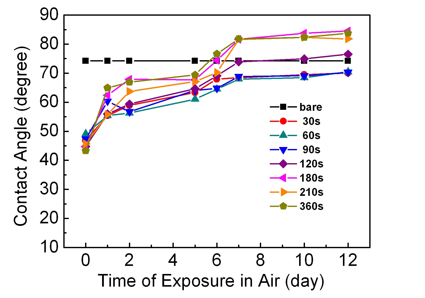
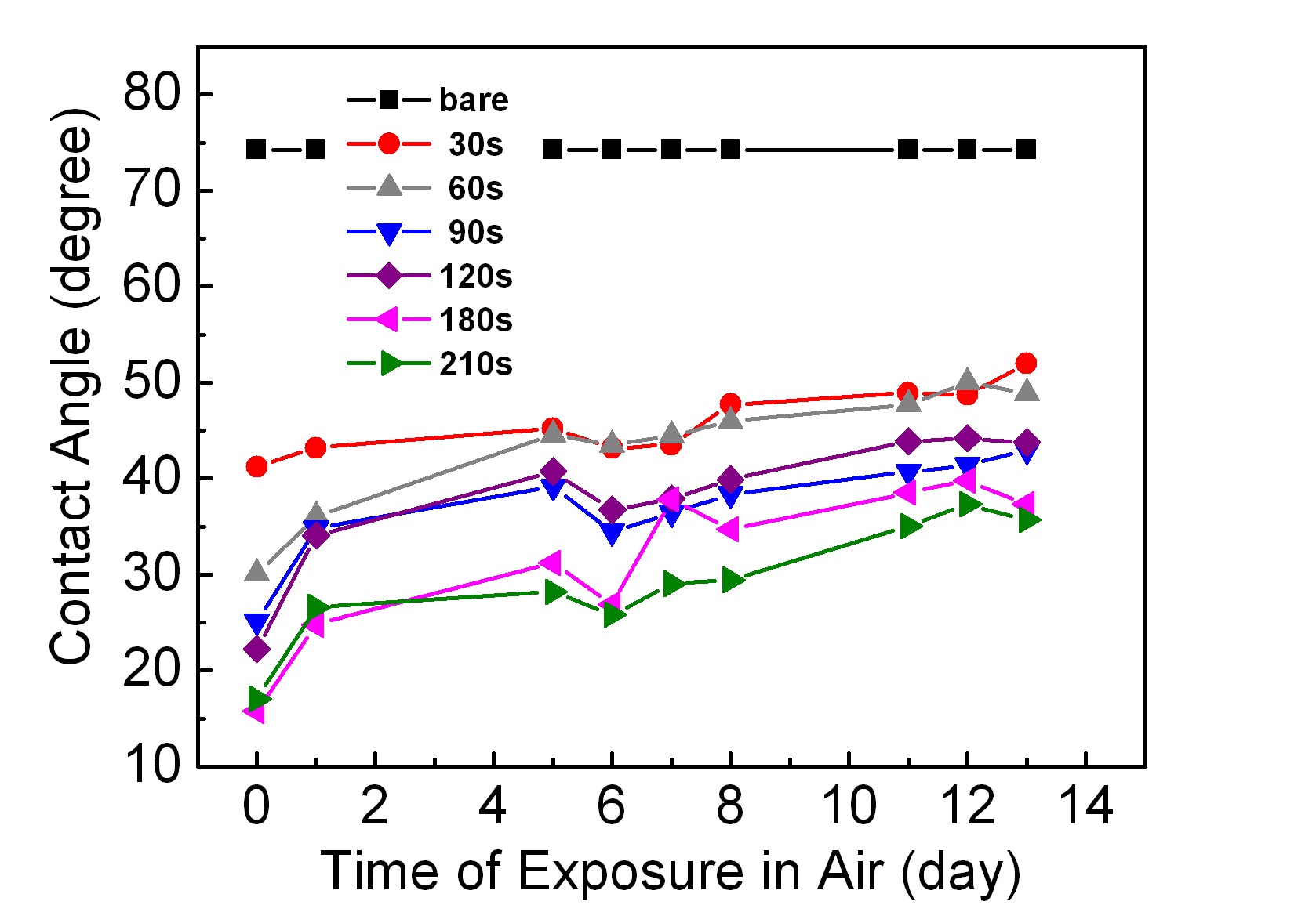
Figure 3 shows plots of contact angle variations with respect to the elapsed time after the chemical etching. Fig. 4 shows the changes in contact angles with the elapsed time after the plasma- induced surface modification process. The contact angle on a bare ABS surface was about 75°.
The contact angles measured immediately after the chemical etching were in the range of 43~50°. As shown in Fig. 3, the chemically etched surfaces did not show any substantial differences in contact angles at the beginning (corresponding to 0 days). This implies that by increasing the chemical etching time, the size and number of holes can be increased, but the hydrophilicity cannot be increased. If the chemically etched samples were left in air for a long time to check for any changes in their contact angles, the values returned to that for bare ABS after 7~8 days. In the chemical etching process, the surface is attacked by acids, so that it becomes unstable, active, and polarized. Therefore, the
mutual interaction strength between water molecules and the chemically etched surface is stronger than before the etching process. Consequently, the contact angle with chemical etching is at first less than that for a bare sample, but the value is restored as time goes on due to stabilization of the etched surface in air.
As shown in Fig. 4, the contact angles just after plasma treatment were in a range of 18~40°, and dependent on the plasma treatment time. If the plasma treatment time was longer, then the contact angle would decrease. All the values were less than those on the chemically etched surfaces, which means that the plasma-treated surface is more hydrophilic. Additionally, the hydrophilicity can be controlled by the plasma treatment time, in contrast to the chemical etching. After leaving in air after the plasma treatment, the surfaces showed variations inct angles, with characteristics that differ from the case of the chemically etched surfaces. The contact angles did not return to the value of the bare sample surface, but seemed to converge asymptotically to 30~48°. This result has important implications with respect to applications, because if the surface morphology does not change with time after plasma treatment, and assuming that the adhesion strength depends only on the morphology and contact angle, leaving the sample in air for a considerable period of time after the plasma treatment will not affect the adhesion strength of the plating.
With increasing etching time, the chemically etched surfaces clearly show larger holes and deeper etched structure. But the prolonged reaction of strong acids can make ABS excessively etched, so that the surface structure, which gives rise to the mechanical strength in adhesion, is mechanically brittle. This means that excessive etching is not desirable for good adhesion of metallic film on ABS. In contrast, the plasma treatment does not show such excessive etching with increasing treatment time. Up to a certain critical treatment time, the number of holes was
increased, and seemed to stop increasing thereafter. The plasma only affected the shallow surface region of the ABS in this experiment. Therefore, excessive etching is relatively less likely in the plasma etching process in comparison with the chemical etching process. The plasma method performed in this study is comparatively better for improving the adhesion by shallow surface treatment.
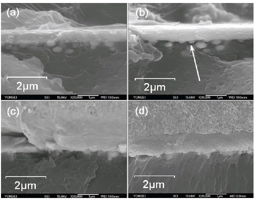
Figure 5 shows cross sectional SEM images of the Ni-plated samples. Holes and Ni metallic grains in the holes can be seen for the samples in both the chemically etched and the plasma-treated samples. The anchoring effect on the adhesion can be seen clearly in the images. The adhesion strength of the chemically etched samples might be better than that of the plasma treated, because metal grains seem to be more distinct, and are located deeper below the surface. However, in Fig. 5(b), a small gap can be found between grains and the ABS, as indicated by the arrow. This is thought to have resulted from the detachment of a metallic grain from the ABS due to the mechanical impact applied during the process of making the cross-sectional specimen. The physical adhesion of the chemically etched samples due to the anchoring effect may be better compared to that of the plasmatreated samples, but the chemical adhesion at the molecular level is not. The plasma-etched samples did not show such a detachment of the coated metal in the cross-sectional images. With this and the results of the contact angle measurements, two main contributions to the adhesion can be considered, one physical and the other chemical. The adhesion strength is a net result of these two factors. Hence, we were able to understand that the plasma-treated samples show better adhesion strength than the chemically etched samples.
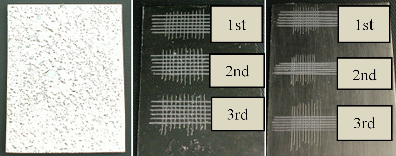
The easiest way to test the adhesion strength is the peel test. As shown in Fig. 6, deep groove lines were first made with a sharp knife through the Ni, penetrating to the ABS and crossing perpendicularly with spacing of about 1 mm. Then, tape (3M 810D) was attached to the Ni-plated samples and peeled off. Thereafter, the number of detached Ni metal pieces per unit area was counted. Within the limit of our experimental conditions, both the chemically etched and the plasma-treated samples showed no detachment. The middle image in Fig. 6 shows a chemically etched sample obtained with an etching time of 210 s. The right image in Fig. 6 shows a plasma-treated sample obtained with a treatment time 120 s. The left image shows an electroless Niplated ABS with neither chemical etching nor plasma treatment after the degreasing process. The Ni film on the surface not subjected to any modification was physically seated-on rather than adhered to the ABS, such that the metallic film could not be flat
and stick to the flat ABS substrate. The film instead appeared as a wrinkled metal film.
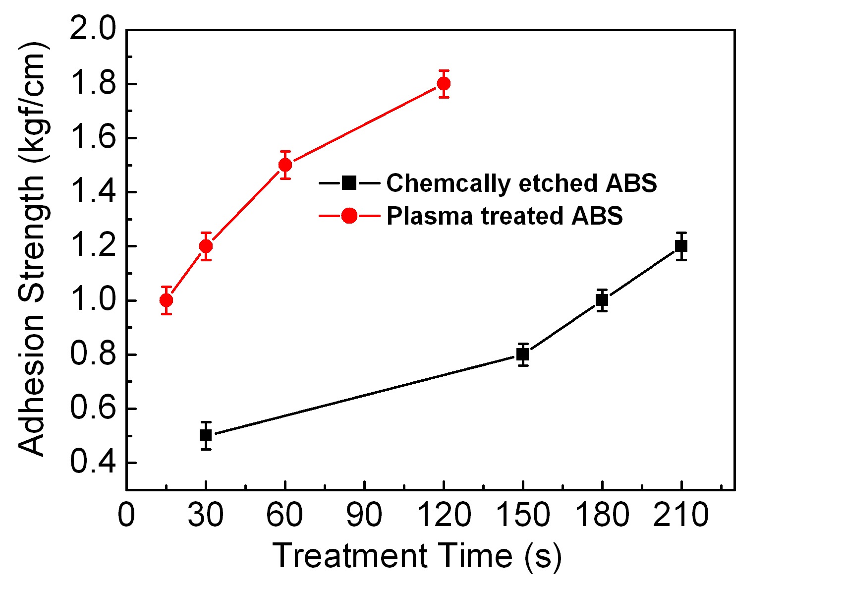
Figure 7 shows plots of the results of the 90° peel-off test. In general, an adhesion strength of 1.2 kgf/cm is regarded as good in the 90° peel-off test. In this study, good adhesion strengths of the samples prepared by plasma-induced surface modification could be obtained with less processing time compared to those prepared by chemical etching. Chemical etching required 210 s to obtain an adhesion strength of 1.5 kgf/cm, but the plasma treatment needed only 120 s to achieve 1.8 kgf/cm. Within the experimental limits of this study, if the times for the surface modification processes were the same, then the plasma treatment method produced results with better adhesion strength.
The thermal stress test was performed only with the samples having adhesion strength more than 1.0 kgf/cm in the 90° peeloff test. All the samples obtained with chemical etching failed to pass the test, but all the plasma treatment samples succeeded. Even though the chemically etched surfaces may have more anchoring sites or holes, the plasma-treated surfaces exhibit stronger adhesion to the metal. The plasma-induced surface modification method seems to be better for improving the adhesion strength and for reducing the number of steps of the plating process. The plasma treated samples are more durable and resist thermal stress. It may be inferred that the improved adhesion strength is not due to physical factors, but to chemical factors. Further study to understand how the adhesion strength is improved in the plasma-treated samples is necessary.
A process of surface treatment for electroless metal plating on ABS plate has been developed. The process reduces the number of processing steps, does not produce acidic waste water, and is environmentally friendly. Also, there is no need for degreasing processes with this method. Using atmospheric pressure DBDs at room temperature in air, surface treatment provides necessary anchoring sites or holes on the ABS surface to enable adhesion. Compared to chemical etching, it is possible to modify only a shallow surface. The appearances of plated samples obtained with both processes are similar. The results of contact angle measurements showed that the plasma-treated surfaces are more hydrophilic. The cross-sectional SEM images and the results of the peel-off tests after Ni plating prove that the adhesion strength of the plasma-treated samples is better. Therefore, it can be understood that the adhesion strength is determined not only by physical binding but also by chemical binding due to the surface hydrophilicity. As an environmentally friendly process, surface modification by atmospheric pressure DBD plasma is appropriate for electroless plating, and produces high-quality adhesion strength of metallic film on ABS plate.