Micro Electro Mechanical switches operating at radio frequencies have been the subject of extensive research over the past few decades. Various designs of RF-MEMS switches, actuated through electrostatic [1-3], magnetic [4], piezoelectric [5], or thermally [6] induced forces, have been successfully implemented in various satellite and defense applications. The most popular among these are electrostatically actuated MEMS switches, due to their near-zero power consumption, very high isolation, very low insertion loss, linearity and low intermodulation products in switching operations [7]. An electrostatic force is generated between the fixed electrode and movable beam, which causes the mechanical movement of the beam above the RF signal line.
Research done in recent years has led to two main types of RF-MEMS switches: fixed-fixed beam and cantilever type. These switches use the elastic property of the beam structure to restore the moving part to its rest position, when actuation force is removed. Attention has been paid to enhance these basic designs in recent years [8]. RF-MEMS switches also have their share of problems, which include insufficient reliability, high actuation voltage, low power handling capability and relatively low switching speeds. Various efforts have been made to eliminate stiction, and achieve high reliability designs of MEMS switches [9].
This paper presents a novel design of an RF-MEMS dc contact switch, providing seesaw-type operation. This eliminates the dependence of the dynamic movement of the switch on elastic recovery forces, and hence requires low actuation voltage, while offering low transition time and high power handling capability.
2.1 Design and principles of operation
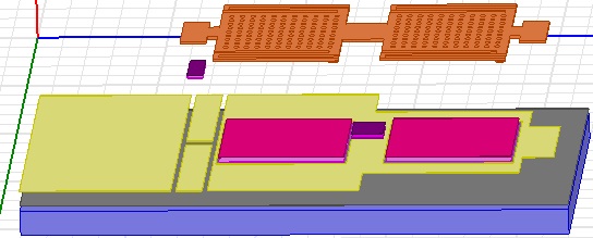
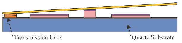
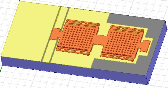
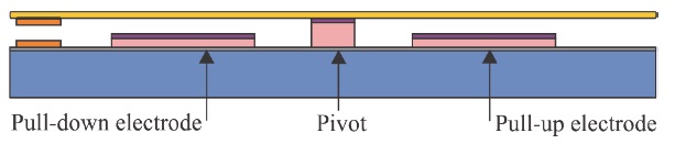
The proposed RF MEMS switch consists of a coplanar waveguide (CPW) line for the RF signal transmission, and electrodes for electrostatic actuation on quartz substrate, as shown in Fig. 1 and Fig. 2. The CPW line consists of a 50 μm wide signal line 10 μm gap between the signal and ground line. The gap between open signal lines is taken to be 20 μm. The membrane rests on a pivot. The pivot is at the center of the membrane, which is used
for the seesaw operation. The membrane is provided with meanders, which result in low values for the spring constant, and easy movement of the membrane.
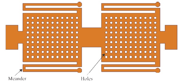
Figure 2 shows individual components of the switch, to provide a clear understanding of the design. The driving electrodes in the same plane as the CPW are covered with a dielectric layer. The contact metal fixed beneath the membrane provides contact with the open signal line, when the switch is actuated. This gold contact covered with dielectric is shown halfway between the membrane and the signal line, for better visibility. The meanders are fixed to the ground plane.
The basic working principle of the proposed switch is based on the rotational movement of a seesaw seesaw-type beam. The movable part rests on top of the pivot, which is placed on the ground plane, and is actuated through two driving electrodes (pull-up electrode and pull-down electrode), causing the seesawtype rotational movement. When no actuation voltage is applied to any of the driving electrodes, the beam is at “rest-state”, as shown in Fig 3(a). When actuation voltage is applied to the pulldown electrode, the switch is activated, and it snaps down on the transmission line, and closes the open ends of the RF transmission line. This is called the “down-state” or “ON-state”, and is shown in Fig 3(b). When actuation voltage is applied to the pullup electrode, the beam rotates as shown in Fig 3(c), and hence the contact metal moves approximately 2 μm above the RF line, which is double the initial gap between the two at the rest-state. This is the “up-state” or “OFF-state”, and results in high isolation. Hence, this design proposes a switch that is stiction-free, and has high isolation.
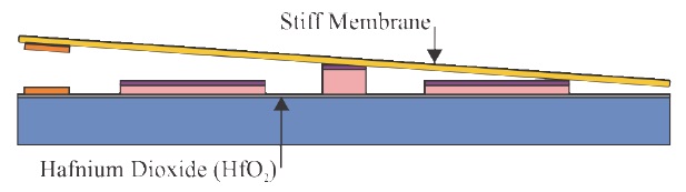
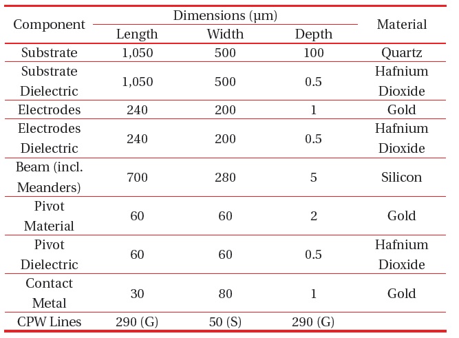
Because of the pivot and 5 μm thickness of the membrane, this 1 μm gap between the contact metal and RF-line is maintained without bending or stiction, making it possible to operate the switch at very low voltage. Table 1 shows the dimensions of various components of the switch design.
2.2 Selection of materials and switch characteristics
The surface of a MEMS switch substrate should be flat and smooth. It should have uniform electrical properties and chemical resistance (as required during fabrication). These requirements make quartz a good candidate, as it possesses all the above requirements, and is cheap.
The actuation electrodes of gold are in the same plane as the CPW line, and are isolated from the beam with a 0.5 μm thick dielectric layer. A high k-dielectric Hafnium dioxide (dielectric constant =25) is used as a dielectric layer covering the substrate and actuation electrodes.
A pivot made of gold is fixed to the ground plane, and a dielectric covering is provided over the pivot. The Si membrane with meanders rests on a pivot, and it is these meanders that fix the membrane strongly to the ground plane, with the help of cylindrical contacts. The beam has a symmetrical structure, as shown in Fig. 4, such that it has equal length from the center of the pivot, which is necessary for the seesaw operation. An array of equally spaced holes is provided in the membrane, to reduce
[Table 1.] Dimensions of the proposed switch design.
Dimensions of the proposed switch design.
the mass of the switch and resistance of the air, so as to increase the speed of the switch. These holes also help in easy removal of the sacrificial layer during fabrication.
Silicon is used for the membrane, as it is robust, and has a low initial stress for bending, compared to Au or Al membranes. Hence, it has no residual stress component, which results in locally different bending of the membrane, and maintaining a constant gap between the membrane and transmission line. Various parameters of silicon material used in the membrane design are given in Table 2.
2.2.1 Actuation voltage and power handling capability
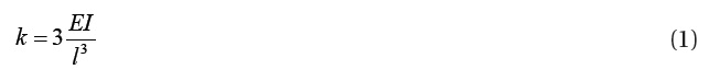
In the proposed design, the spring constant is approximated, assuming that the membrane does not bend, and hence provides the concentrated load at the ends. Since the Si membrane is not fixed at the ends, any residual stress within the film is released, and the spring constant does not contain a residual stress component. The spring constant is given by [8].
where, the moment of inertia, I is further calculated as:

The Actuation voltage Vp, of the DC-contact seesaw type switch design with spring constant,
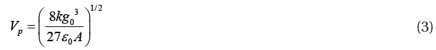
where, ε0 is the permittivity of free space, g0 is the gap between the membrane and the electrode, and A is the area of the driving electrodes. The calculated value of the actuation voltage is 6.43 V, for the dimensions of the switch as given in Table 1. If the spring constant and permittivity are fixed, then the value of the actuation voltage completely depends on the gap between the electrode and the membrane.
The power handling capability is augmented in relation to other designs, due to the use of a pull-up electrode, as the switching operation does not rely on the elastic recovery force of the beam. This design counteracts the hot switching effect at high power applications.
2.2.2 High isolation and stiction-free operation
In the proposed switch design, elastic recovery force is not used to restore the membrane to its rest position; instead the movement of the membrane depends on the driving force applied by pull-up and pull-down electrodes. The actuation by these electrodes provides the transition between the OFF-state and ON-state. Moreover, in the OFF-state the gap between the contact metal and the open transmission line is double that in the rest state, due to the rotational movement of the beam. Hence, good isolation is provided in the OFF-state.
DC-contact switches depend on the contact and separation of surfaces for their functionality. Hence, various surface forces like Capillary and Van der Waals forces come into action, and interfere with the switching operation [14]. Moreover, the induced heating proportional to the RF signal power passing through the contact may cause contact micro-welding, leading to stiction. This is a major reliability concern in metal contact switches. In the proposed switch design, a separate pull-up electrode is used,
[Table 2.] Parameters of the silicon membrane.

Parameters of the silicon membrane.
which provides an actuation force to overcome such forces, and to separate the surfaces. Hence, the seesaw-based operation of the switch provides high reliability.
The dynamic model of membrane-type RF-MEMS switches [12,13] considers the effects of the squeeze-film air damping, the bouncing of the switch and the etch holes in the membrane.
The dynamic model taken here considers the rotational movement of the seesaw-type beam, the absence of the elastic recovery force, and the effect of squeeze-film air damping in the two states of operation of the switch [11].
The membrane is provided with holes to reduce the air damping effect, hence increasing the transition speed of the switch.
3.1.1 Electrostatic torque function
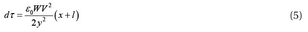
The electrostatic torque function τ(φ,V), is obtained by multiplying the elementary electrostatic force with the distance to the rotational axis, and then this expression is integrated over the electrode length (

3.1.2 Rotational motion of membrane
If,

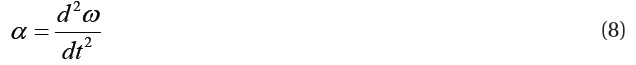
The angular velocity ω is given by:

The expression for angular acceleration α is:
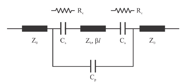
The electromagnetic model of the switch can be approximated with an equivalent C-L-R circuit model, as shown in Fig. 5. Cs is the series capacitance between the metal contact and transmission line, Rc is the contact resistance, and
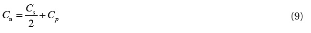
3.2.1 Up-state capacitance
The up-state capacitance is composed of (a) series capacitance (Cs) between the T-line and switch metal, and (b) parasitic capacitance (Cp) between open-ends of the T-line [8].
The total up-state capacitance of the DC-contact seesaw switch with two contact areas is:
The series capacitance, Cs is composed of a parallel-plate component (Cpp=εA/g), and a fringing component, which is around 30-60% of Cpp. If one neglects the high impedance transmission line between the contact areas in the model shown in Fig. 5, the isolation can then be calculated as:
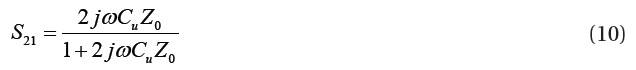
For S21<<-10 dB and 2ωCuZ0<<1, we have;

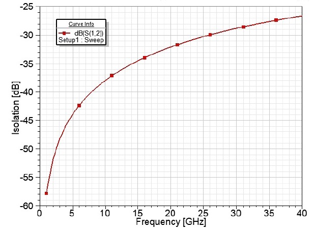
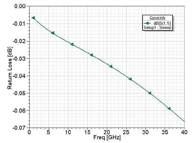
Equation (11) gives a straightforward determination of the up-state capacitance from the measured isolation data. The isolation
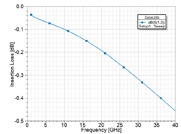
and return loss, at frequencies ranging from 1 GHz to 40 GHz, are obtained by using Ansoft HFSS version 13, as shown in Fig. 6 and Fig. 7 respectively.
3.2.2 Down-state resistance and inductance
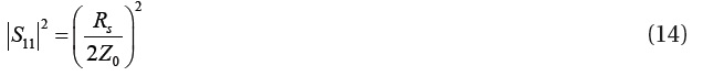
In this proposed DC-contact MEMS series switch, the length and width of the contact metal determines the resistance between the contact areas (Rc). Further, the T-line loss (Rl) and equivalent resistance (Rs1) must also be added. The total switch resistance for the two contact areas [8] is:

The switch resistance can be determined from the measured loss in the down-state position. The equivalent series impedance of a dc-contact switch in the down-state position is:

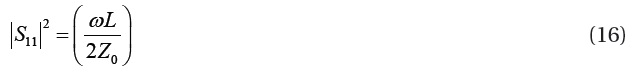
For Zs= Rs, (ωL << Rs), we have:
The down-state inductance of this switch design can be extracted from the measured S11 values. The switch impedance and reflection coefficient are:

The plot for insertion loss, as calculated using Ansoft HFSS version 13 for frequencies ranging from 1 GHz to 40 GHz, is as shown in Fig. 8.
The proposed design utilizes a novel seesaw-type structure to overcome the stiction problems in MEMS switches, due to insufficient elastic recovery force in the membrane, it possessing high
voltage. The transition time to the down-state is reduced for the same actuation voltage, due to the absence of any counteracting elastic force. Another advantage of this switch design is the improved power handling capability, due to the presence of the pull-up electrode.
The measured RF response is excellent, and shows that the proposed design is suitable for applications where low power consumption is essential, such as wireless components and space systems.